
- Main Product Image:
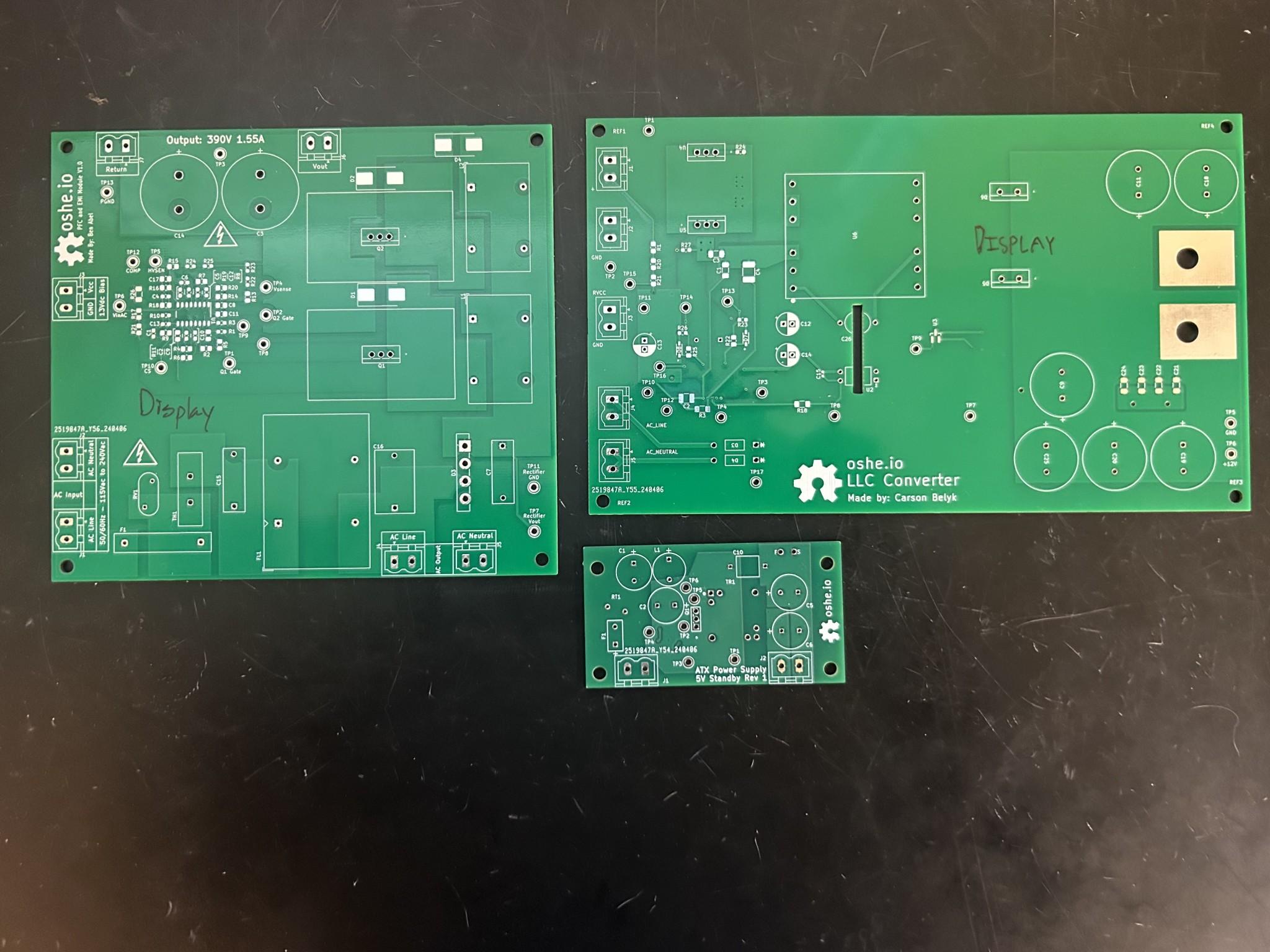
Figure 1: Pictures of Alpha Prototype PCBs
- Project Description:
- ATX Power Supply is sponsored by Plexus with the goal of designing and prototyping an open-source, high-powered ATX power supply. Our first prototype is split up into 3 printed circuit boards (PCBs): EMI filtering & PFC, LLC Converter, and DC-DC Converter. These PCBs are made larger than the ATX form factor to provide ample space for the testing and debug phase.
- Further documentation can all be found in our osf.io repository https://osf.io/ekn2q/
- Methodology in Brief:
- PFC and EMI
- Beginning with the generic interleaved boost PFC topology, seen in figure X, as specified by the UCC28065 datasheet, the first step was to identify what real values and real components would be needed to meet the desired specifications. This process and the choices made to select and choose these passive and active components is fully laid out in EMI and PFC Schematic Overview, but with the help of a supplied TI excel design calculator the required resistances and capacitance values could be identified.
- PFC and EMI
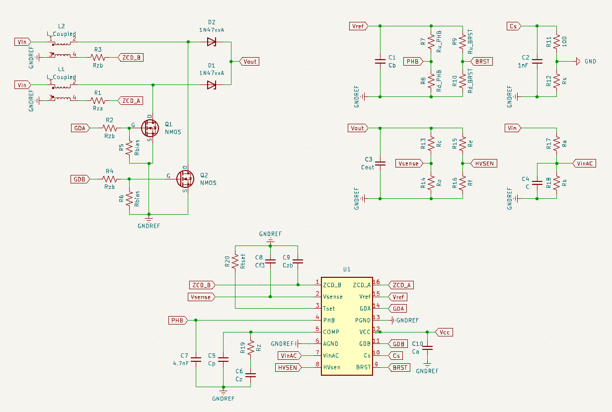
Figure 1: Generic PFC Topology
- After working through the design calculator and finding the exact values needed for the multiple resistor dividers and parameter setting resistors and capacitors, real components matching as close as acceptable were found on Digikey. These real components were added to the schematic, updating them with the proper footprint and added to a BOM to make parts purchasing easier in the future.
- The other components which weren’t explicitly determined through the design calculator such as the active components like the MOSFETs and Diodes where selected based on further design calculations, specified in EMI and PFC Schematic Overview, in conjunction with referencing the UCC28064 Eval board.
- After a majority of our components were selected, we met and sent off our schematics to our sponsor for a schematic review. This fresh set of eyes on our design would aid in trying to find any issues or considerations we have missed.
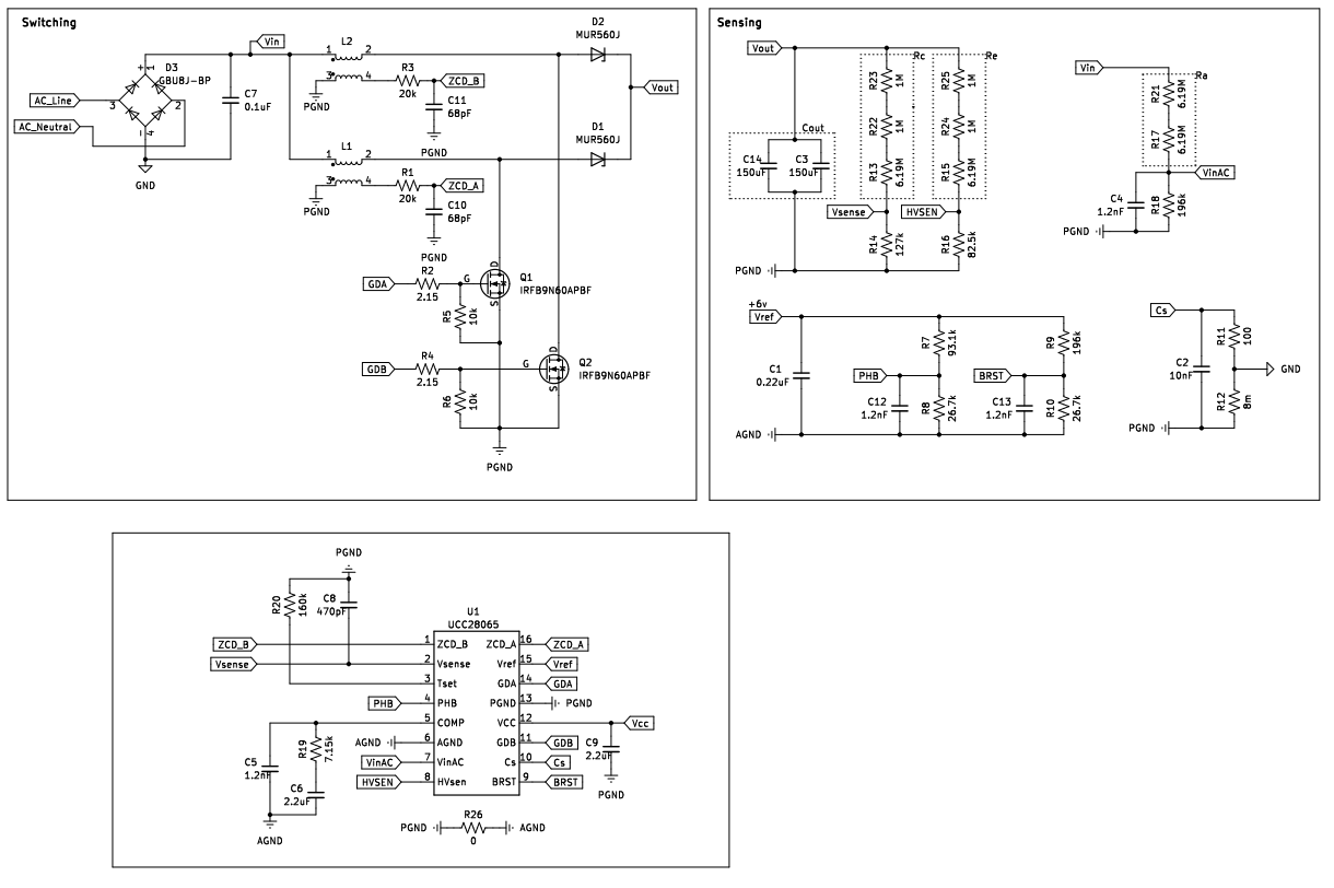
Figure 2: PFC Schematic Design With Real Components
- While waiting for feedback for the schematic review, we knew we were missing the EMI filtering for the AC wall input, so work began on that. Much of the EMI design came from referencing the UCC28064 eval board. The components referenced from the eval board, which only has a 300 watt rating were appropriately sized for out 600 watt design.
- Along with this we began working on our layout design, getting a rough idea of component location and routing some of the low voltage resistor divider networks around the IC.
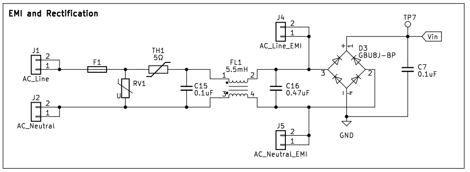
Figure 3: EMI Schematic Design With Real Components
- After getting feedback from our schematic review, we made the recommended changes that our sponsor gave to us. Some of these recommendations included general schematic clean up, as well as the addition of a flyback diode, which was present in the eval board, but not in my current schematic.
- Other changes that we had decided on regarding layout design was shifting to a four layer board instead of two. This would give us the added benefit of running signal and low power traces in the middle layers leaving the top and bottom for the high power traces.
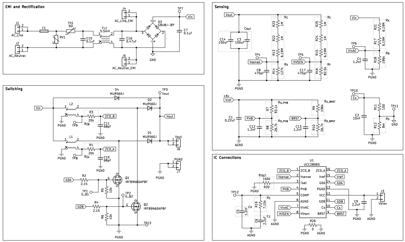
Figure 4: Final PFC and EMI Schematic Design
- Finishing up layout design, we met with our sponsor to validate that our layout was proper and there weren’t any overarching issues that we had missed. We ensured that on all the high voltage rails that proper clearance was had to ensure that there wouldn’t be any issues with arcing.
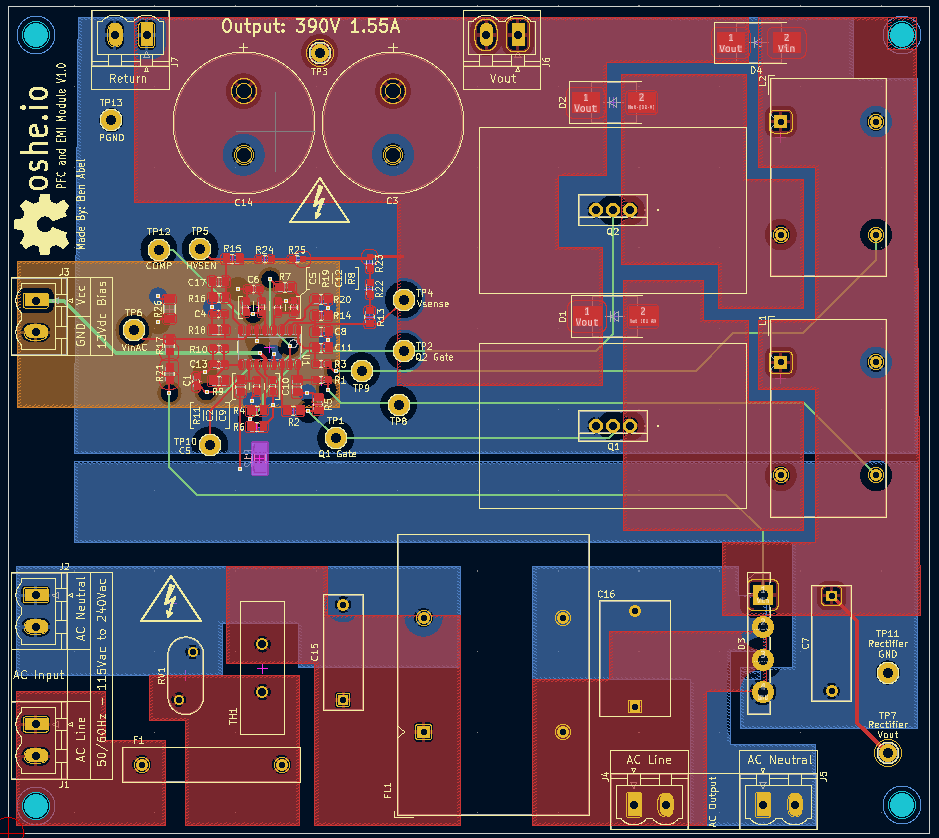
Figure 5: Final PFC and EMI PCB Design
- LLC
- Starting from the generic LLC topology, the first step was to find real values for passive and active components. Step one was to start working through the supplied TI excel calculator for our selected IC to find values for various components. These components include output capacitors, input voltage resistor dividers, current sensor capacitors, and other components that are mentioned in LLC System Overview.

Figure 6: Generic LLC Topology
- As these component values were found, real versions were found on DigiKey and added to both the schematic with value and footprint, and the BOM so we could easily bulk order parts later. Some specifics such as the feedback circuit started to become more flushed out and a framework was drawn out to allow for further design and changes to be made later during testing. Other blocks such as the HV Startup diodes and resistors were chosen based upon the datasheet for the UCC256404 and the eval board.
- More output capacitors were also added as output ripple current ratings need to be taken into account to meet the targeted ripple spec of 102mV

Figure 7: LLC Schematic with some real components
- For small passives such as SMD capacitors and resistors, the ability for rework was considered so components no smaller than 0603 were generally considered. Most other components are 0805 or larger except for C6, C7, and C15 which needed to be smaller due to space constraints or footprint limited due to desired component values.
- Most major components have been finalized at this point and a schematic review with our sponsor was carried out to get an outside pair of eyes on our designs to try and find any issues or considerations we have missed.

Figure 8: LLC Schematic with more components
- While waiting on feedback for our schematic review, we moved forward.
- into PCB layout since our major components were finalized. Considerations were starting to form for connecting the boards together, the ampacity and acceptable temp rise of our main power paths, and even adding test points to the system.
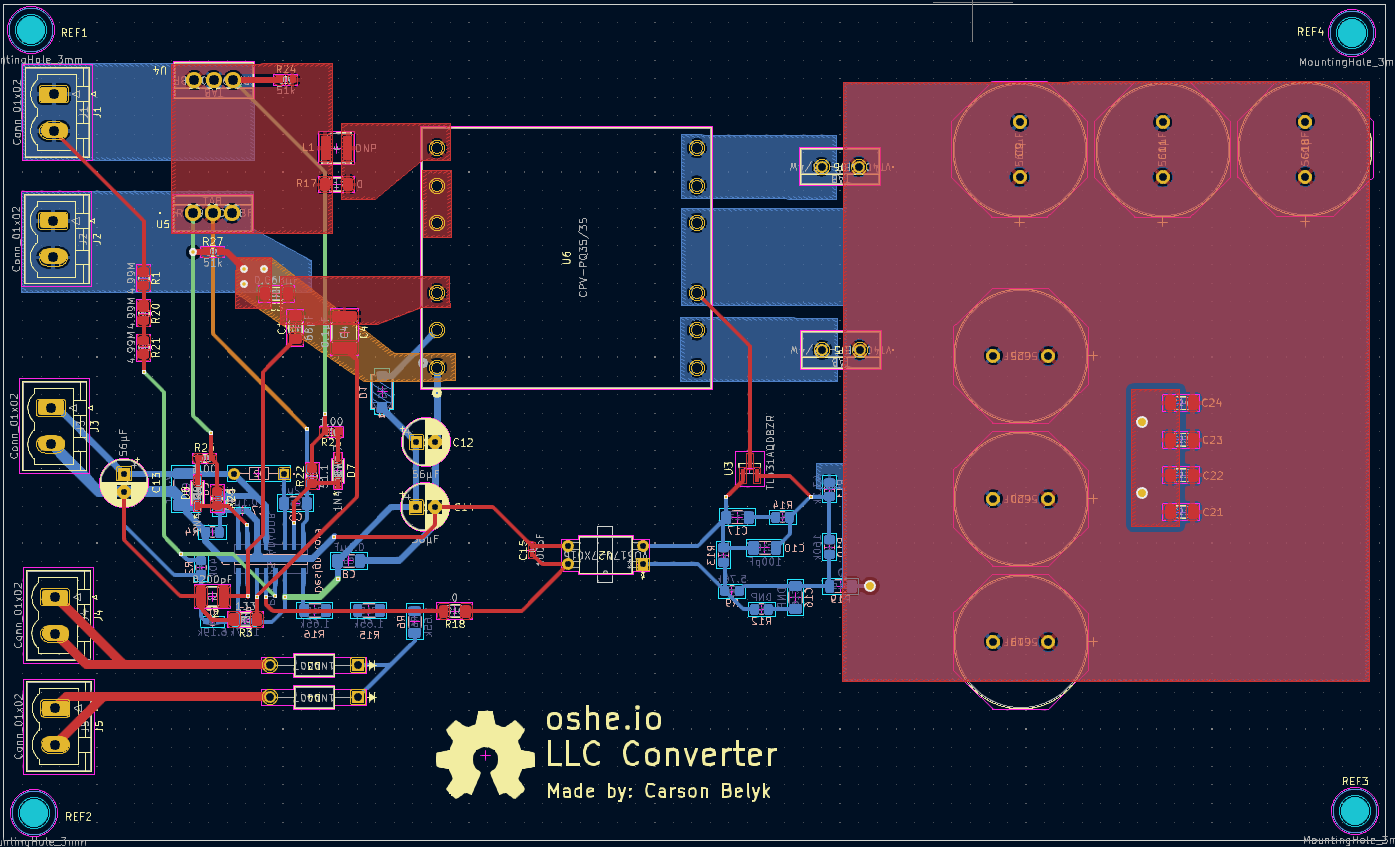
Figure 9: Initial PCB Design
- Once we received Schematic feedback, final schematic changes were made and general schematic cleanliness was refreshed for readability. At this point we got extra feedback for our PCB layouts as well so we could readjust while updating our PCB layouts from our schematic review. This would include adding RCD clamps and gate resistors for the MOSFETs and changing some traces to pours.
- The largest modification would be shifting to a four layer board to have signal/low power traces run on inner layers while the main power paths remain on the outer layers. This has the additional benefit of allowing for sandwiching of ground planes around sensitive traces where applicable.
- Extra modifications to this layout include output pads for terminal connectors capable of the max output current and leaving ample room for the heatsink selected for the FETs and Rectifying diodes.

Figure 10: Final LLC Schematic
- We then had a final PCB Layout review before ordering our boards and made a few edits to our boards then ordered both them and our parts.
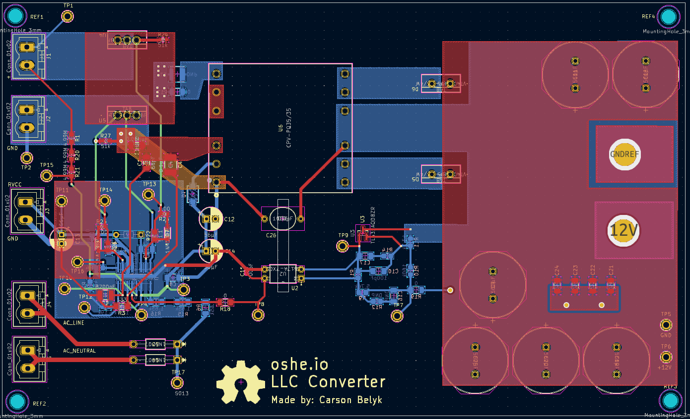
Figure 11: Final LLC PCB Layout
- 5 V Standby
- When a desktop PC is turned off so is its power supply. That means that the 12 V, 5 V, 3.3 V, and -12 V rails are all at 0 V and they won’t supply any power to the computer. When you want your computer to turn on and you push the power button on your PC case, the computer sends a signal to the power supply to tell it to turn on. You might notice an issue here . . . If the power supply is off, where is the computer supposed to get power from to tell the power supply to turn on? That’s where the 5 V standby rail comes in! The primary purpose of the 5 V standby rail is to efficiently supply some small amount of power to the computer motherboard all the time so the motherboard can tell the power supply to turn on the main power rails.
- For our 5V standby rail we have a few requirements and goals that we had to meet. We need to produce 5 V at up to somewhere around 2 A. We also wanted to keep the 5 V standby converter fairly simple, using relatively few components and an off-the-shelf transformer.
- To meet these requirements we chose to use the traditional flyback converter topology. We initially chose to use the UCC38C42 flyback controller, but we had trouble sourcing a suitable transformer. While searching for a transformer we ran across an evaluation board for the UCC28704 flyback controller (UCC28704EVM-724). The evaluation board we found is capable of producing 5V at 2A which is suitable for the 5V standby rail of an ATX power supply. The UCC28704 datasheet provides good documentation on how to design a functional flyback converter with the UCC28704, but designing a flyback converter that works well is still a complex task. Due to this we opted to heavily base our initial 5V standby design on the evaluation board. The transformer used in this evaluation board is also available from Würth Elektronik, so we don’t need to design our own.
- Our schematic (Figure 12) is largely a carbon-copy of the evaluation board from TI. The UCC28704 chip has an integrated MOSFET driver that switches Q1, which pulls current through the primary of the transformer (top left of TR1). The duty cycle is varied to control the voltage on the secondary of the transformer (right side of TR1). The UCC28704 is initially powered through the three 5.11 MΩ resistors. After startup it begins drawing its power from the auxiliary winding of the transformer (bottom left winding of TR1).
- One slight oddity of the UCC28704 is that it uses primary-side feedback instead of the more common secondary-side feedback. Typically on isolated power supplies you see a little optoisolator connecting a bunch of circuitry on both sides of the transformer so the controller IC (typically on the primary side of the transformer) can see what the output voltage is. On our schematic (Figure 12) you can see that there aren’t any components going between the primary and secondary sides of the transformer except the Y capacitor C10 which is for EMC purposes. The UCC28704 is designed to regulate the output voltage based on what it can measure on the primary side of the transformer. This eliminates the need for an optoisolator, reducing component count and therefore cost.
- The layout is fairly close to that of the evaluation board. One thing to note on the layout is that the secondary winding comes out of the transformer as loose wires that get soldered to the board, near the upper right corner of the PCB.
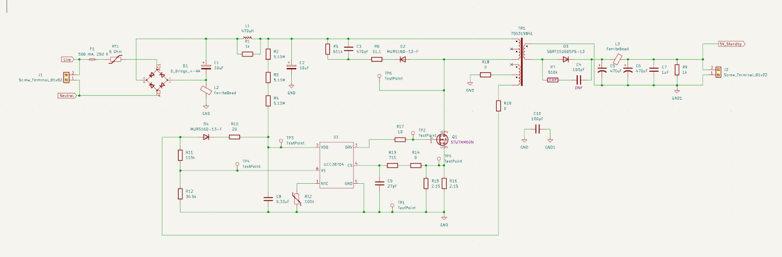
Figure 12: Final 5 V standby schematic
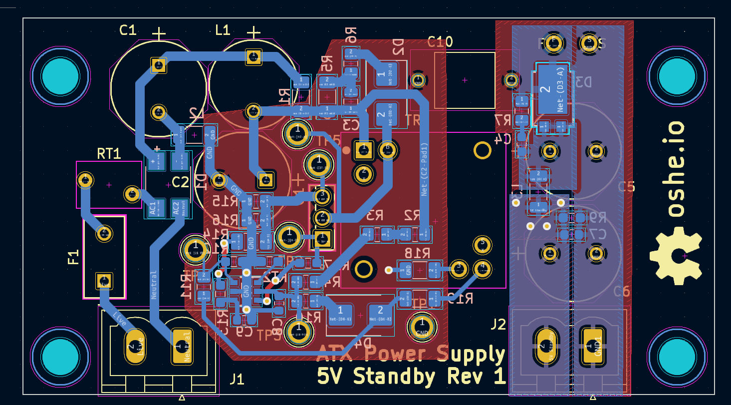
Figure 13: Final 5 V Standby PCB Layout
- 3.3 V Conversion
- The ATX power connector requires a 3.3 V rail utilized by the motherboard for various logic, sensing and power delivery purposes to components on the motherboard as well as peripheral boards.
- As per the standard universally accepted parameters for quality ATX power supplies, the 3.3 V rail will only usually account for about 25% or less of the total current draw from the PSU. For a 600 W unit, with power draw headroom as seen from industry standard ATX power supplies, the 3.3 V rail should have a maximum current output of around 25 A.
- As with the other subsystems in the power supply, a Texas Instruments IC would be sourced to be used as the main control IC due to the extensive available documentation and tools for TI chips. In order to choose a specific IC, the amperage limit was the main constraining factor, as well as the required voltage variance tolerance from the input to the converter and output.
- As per the Intel ATX specification, the 3.3 conversion circuit should be able to accept 11.2 – 12.6 Vdc and output 3.3 V ± 5%.
- Given these specifications, The Texas Instruments TPS548C26 Buck Converter IC was chosen to be used as the main conversion chip for the 3.3 V rail.
- Using TI’s design guidelines for this buck converter IC, the necessary values for the resistors, capacitors and inductor were calculated so that schematic design could begin.
- 3.3 V Converter Test Plans
- Use DC Multimeter to verify various important voltage drops on the board
- Given a 12 V input voltage, compare output voltage to the 3.3 V target voltage with a small load
- Repeat test with a larger load to ensure the maximum output current is sufficient
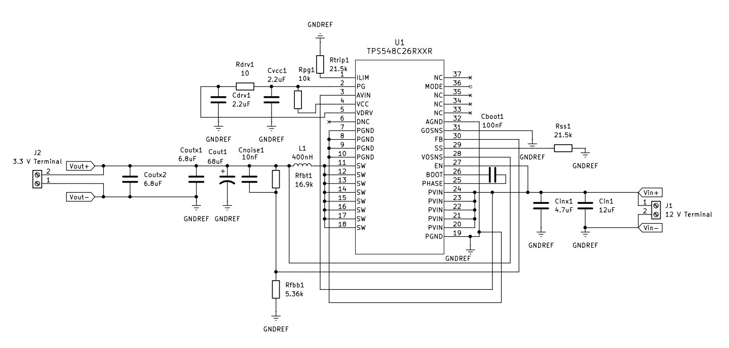
Figure 14: Final Schematic for 3.3 V Conversion Circuit
- 5 V Conversion
- Like the 3.3 V rail, the ATX power connector also requires a 5 V rail that is used for various logic, power delivery and sensing applications on the motherboard and peripheral boards attached to the motherboard.
- The methodology used to design the 5 V converter was very similar to the process used for the 3.3 V converter due to its comparable requirements of usually accounting for another 25% of the total current draw for ATX power supplies. Given this, an equal maximum output current to the 3.3 V converter was chosen for the 5 V converter (25 A).
- As with the maximum output current rating, the output and input voltage variation are the same 11.2 – 12.6 Vdc input and 5 V ± 5% output.
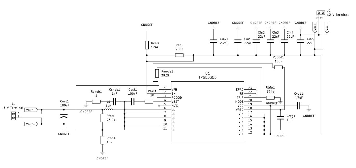
- Considering these constraints, a Texas Instruments buck converter was also chosen for the 5 V converter. For this subsystem, the Texas Instruments TPS53355 Buck Converter IC was selected.
- Again, using TI’s design guidelines for this specific buck converter, the necessary values for the resistors, capacitors and inductor were calculated so that schematic design could begin.
- 5 V Converter Test Plans
- Use DC multimeter to verify various important voltage drops on the board
- Given a 12 V input voltage, compare the output voltage to the 3.3 V target voltage under a small load
- Repeat test under a larger load to ensure maximum output current is sufficient
Figure 15: Final KiCad Schematic for 5 V Conversion Circuit
- -12 V Conversion
- The -12V rail is used to power PCI ports. This is considered legacy technology and integrated to satisfy backward compatibility in the ATX standard.
- The -12V Inverting Buck-Boost (IBB) topology uses a synchronous buck converter IC (LMR33630CRNXR) to invert the 12V coming from the LLC resonant converter to -12V. This is done by grounding the output pins of the synchronous buck converter and connecting the IC’s AGND and PGND pins to the -12V output. This configuration is less energy efficient and causes more voltage stress due to the discontinuous, fast-transitioned currents but is simplistic and compact in design. Shown in the figure below is an example of the signal waveforms of an IBB converter.
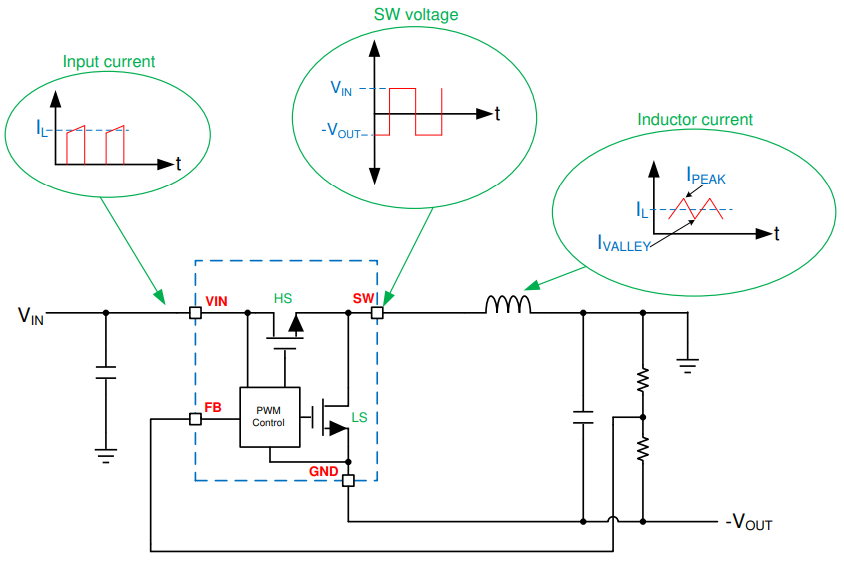
Figure 16: Signal Waveform of IBB Converter
- The IBB circuit sees the input voltage and output voltage whereas a typical buck converter would only see voltages from the input to ground. In this case, the max voltage the circuit experiences is then Vin + |Vout| which is 24V. To account for this voltage stress, all components should be rated for 24V or higher.
- The first iteration of the circuit was using the SOIC package IC on a two-layer board with larger components.
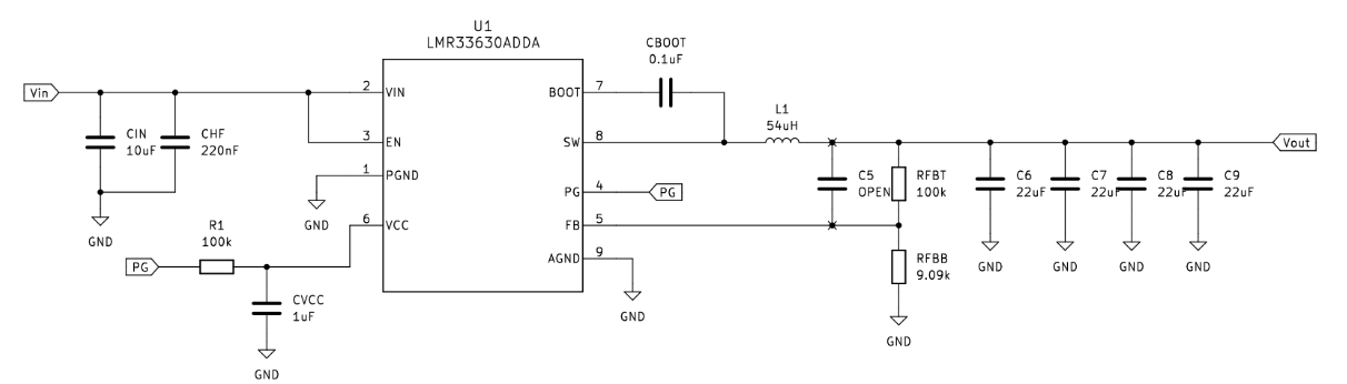
Figure 17: LMR336 SOIC Schematic
- After more considerations regarding the future of this subsystem, the system was transitioned to a four-layer board to be compatible with the other boards. This opened up the opportunity to use a smaller footprint VQFN package size which would take up less board space and make reaching the goal of fitting the PCBs into an ATX footprint easier.
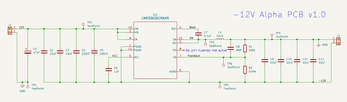
Figure 18: LMR336 VQFN Schematic
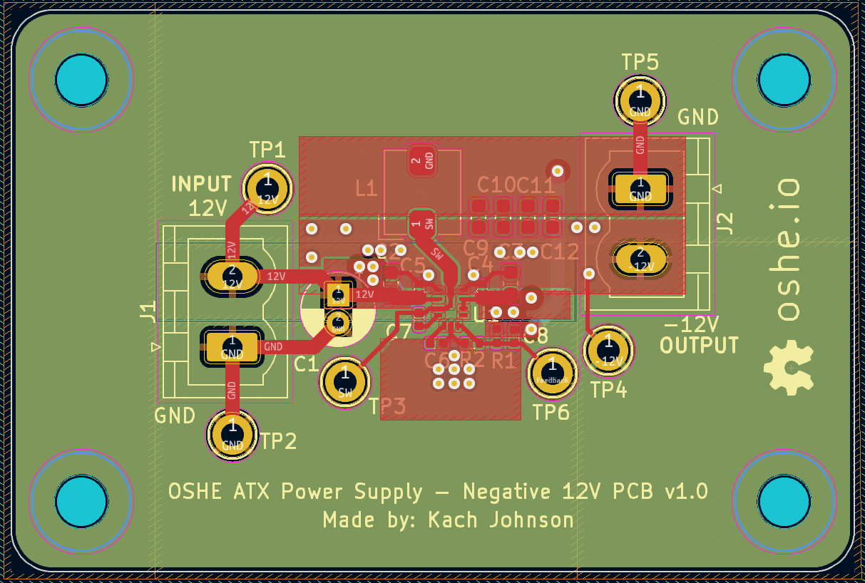
Figure 19: -12V PCB Layout
- In the final iteration, large test points were added at critical locations to make testing easier.
- Bill of Materials (BOM):
- Our project bill of materials is located at our OSF repository here (https://osf.io/ekn2q/)
- Unit Costs
Looking at the unit cost for each subsection, the prices given for the parts section is enough to populate one board. However, because of the small number of parts and lower cost that can be achieved through greater quantities, specifically with passive components, these prices aren’t an absolute true representation of the overall unit costs. When ordering boards, the minimum order quantity, at least through JLCPCB, where we got them manufactured is 5, so these overall costs are not a direct price correlation to what it would cost to make and populate a single board.
| Subsection | Parts Unit Cost | Board Unit Cost | Digikey Parts List |
| 5V Standby | $14.61 | $0.4 | Link |
| PFC and EMI | $49.45 | $13.32 | Link |
| LLC | $68.75 | $13.64 | Link |
| -12V Converter | $5.88 | $10.91 | Link |
- Tools Used:
- Hardware Tools
- Note about equipment obtainability –
- Several of the tools we used for assembly were high-end SMD (Surface Mount Device) rework tools. We used them to save time during assembly. We’re confident that our boards can be assembled without any or all of the SMD rework tools that we used, but assembly could take longer. Another option is to have the SMD components assembled by JLC PCB. We opted to not go this route to save some money, but it would save a lot of time in assembly.
- PCB Stencils
- We ordered solder paste stencils along with our PCBs to make assembly easier. These are typically metal sheets with holes for each SMD pad on your board. You can put solder paste on the stencil and squeegee it across and you’ll wind up with just the right amount of solder paste on your pads.
- [Picture of stencil/using stencil, will be added after we do assembly]
- Pick and Place Machines
- We had access to manual pick and place machines to aid with assembly. These allow you to pick up components and easily place them on your board. All components can also be placed with tweezers, but it would be even a little bit more tedious.
- [Picture of pick and place machine, will be added after we do assembly]
- Solder Reflow Oven
- We also had access to a solder reflow oven which shaped how we chose to assemble our boards. Our boards could be assembled by hand with solder wire, a soldering iron, and a good pair of tweezers. We also could have gotten them assembled by JLC PCB. We opted to use the reflow method to save money over having JLC PCB assemble our boards while also saving some time over soldering everything by hand. Any solder reflow oven that our boards fit in could be used. If no such oven is available a solder reflow hotplate or a hot air gun could also be used to reflow the boards.
- Microscope Inspection Cameras
- Once again, we had an AmScope inspection microscope available to inspect for solder bridges. If no inspection microscope is available a magnifying glass can also be used and would likely be just as effective.
- Soldering Irons
- We used a soldering iron to touch up any solder joints that were either bridged or didn’t get enough solder during reflow. We also used a soldering iron to solder all of our through-hole components to our boards. Our lab has Hakko FX888D soldering irons, but any temperature controlled soldering iron with a small tip would do.
- [soldering iron picture, will be added after we do assembly]
- Note about equipment obtainability –
- Software Tools
- Gantt Chart for Forecasting
- We used a Gantt chart made in google sheets to do our project organization. There are many Gantt chart templates available online for both Google Sheets and Excel.
- KiCad EDA for Schematic and PCB Layout
- All schematic capture and PCB layout was done in KiCad. This is a free and open source software suite that can be used to do everything from schematic capture to layout to gerber generation/verification. The interactive HTML BOM plugin was also used to assist with assembly.
- TI Webench Power Designer
- TI Webench Power Designer was used to generate initial designs for several portions of our power supply. This is an online tool provided by Texas Instruments that generates power supply designs to meet your requirements.
- Gantt Chart for Forecasting
- Hardware Tools
- Characterization Data:
- Moving forward, these are the tests that will be performed once alpha boards have been assembled to verify their operation
- LLC Feedback Loop Verification
- LLC Oscilloscope testing (for ripple testing) & analysis, does it meet ATX standard?
- Multimeter voltage verification on all output voltages for alpha boards
- Multimeter voltage verification on all subsystem test points on alpha boards
- Ensure output voltage variation in 12 V output meets ATX standard
- Moving forward, these are the tests that will be performed once alpha boards have been assembled to verify their operation
- Sponsors/Acknowledgements:
- Plexus Corp.
- Financial sponsorship
- Christopher Bousho
- Engineering Support
- Plexus Corp.

Figure 20: Plexus Company Logo
- References:
- List of TI whitepapers used per subsection
- 5V Standby
- Using the UCC28704EVM-724 10-W USB Adapter: https://www.ti.com/lit/ug/sluubf1/sluubf1.pdf?ts=1708202842231&ref_url=https%253A%252F%252Fwww.ti.com%252Ftool%252FUCC28704EVM-724
- UCC28704 Datasheet: https://www.ti.com/lit/ds/slusca8a/slusca8a.pdf?ts=1708286118900&ref_url=https%253A%252F%252Fwww.ti.com%252Ftool%252FUCC28704EVM-724
- PFC
- Power Factor Correction (PFC) Circuit Basics: slup390.pdf found on TI website from PSD Seminar
https://www.ti.com/seclit/ml/slup390/slup390.pdf
- UCC25640EVM-020 Evaluation Module User Guide: https://www.ti.com/lit/ug/snvu587a/snvu587a.pdf
- Convert UCC28064A EVM to Higher Switching Frequency Using UCC28065:
https://www.ti.com/lit/an/sluaa28/sluaa28.pdf
- UCC28065 Datasheet: https://www.ti.com/lit/ds/symlink/ucc28065.pdf
- LLC
- Designing an LLC Resonant Half-Bridge Power Converter: slup263.pdf found on TI website from PSD Seminar
- UCC25640EVM-020 Evaluation Module User Guide: https://www.ti.com/lit/ug/sluubx3b/sluubx3b.pdf
- Feedback Loop Design of an LLC Resonant Power Converter: https://www.ti.com/lit/an/slua582a/slua582a.pdf?ts=1712938697991&ref_url=https%253A%252F%252Fwww.google.com%252F
- UCC256404 Datasheet: https://www.ti.com/lit/ds/symlink/ucc256403.pdf?ts=1712904893134&ref_url=https%253A%252F%252Fwww.google.com%252F
- 3.3V Conversion
- 5 V Conversion
- -12 V
- List of EVAL boards used
- PFC Eval Board: https://www.ti.com/tool/UCC28064EVM-004
- LLC Eval Board: https://www.ti.com/tool/UCC25640EVM-020