
Prepared By: Stephen Metcalfe, Luc Prisby, and Luke Janitch
Spring 2024
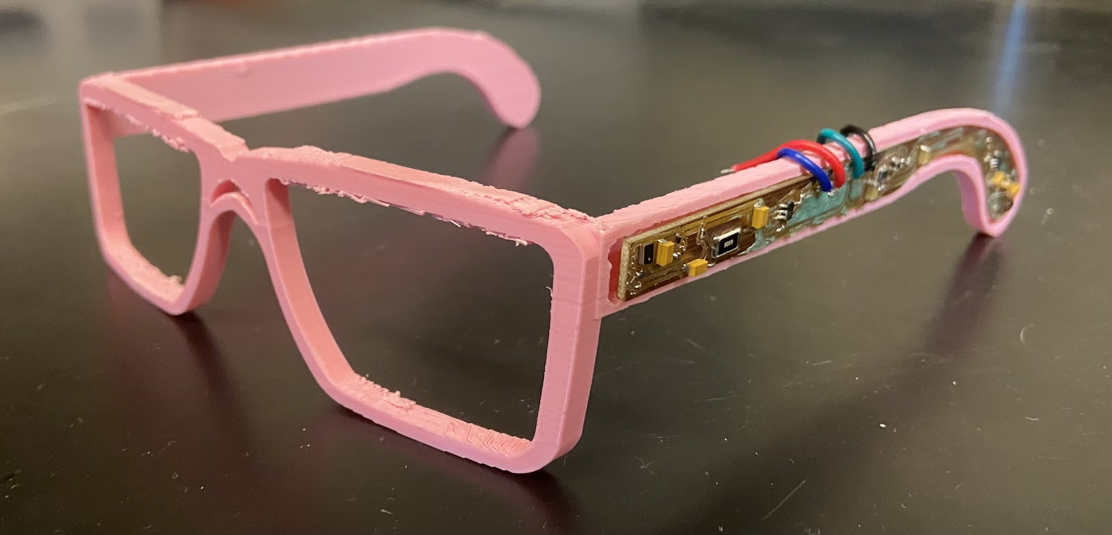
1. Main Product Image
2. Project Description
The goal of the project is to create wearable technology that can display real-time subtitles from the environment to the user. This project may be useful for people who are deaf or hard of hearing. Furthermore, when used in conjunction with live translation, it may help people of different languages communicate effectively.
The main technology behind this project is a carefully placed array of microphones, a small camera and a smart glass display for the user. The idea behind this selection of components is to use the microphone array to hear sounds from an environment, record precise time stamps and intensity measurements, and compare these differences to localize a sound in an environment, much like how human ears work to localize sound [1]. In conjunction with the microphone array, a camera is used to assist identification of sound sources. Using open-source facial tracking software [2], the device will be able to identify possible speakers and combine this with data from the microphone array to come up with robust predictions of the origins of sound. Open-source speech-to-text software will be used to transcribe audio from the environment [3], and a smart glass display will then be used to display in text what a speaker is saying, or a description of certain sounds from an environment, much like subtitles from a TV show or video game.
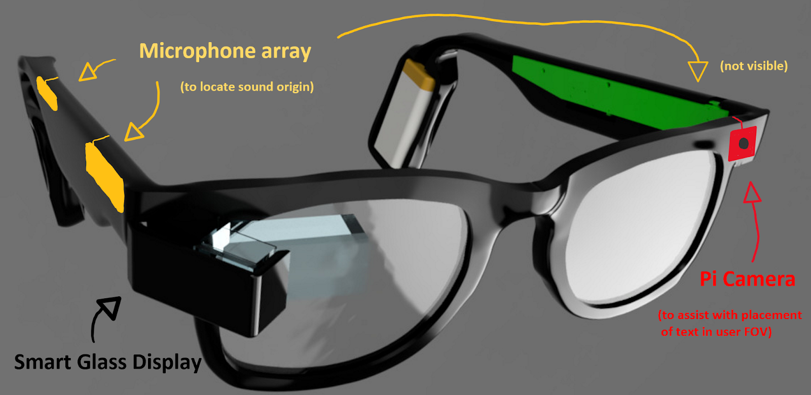
Figure 2: An example of a variation of the final product
Although a smart glass solution is integral to the final design of the product, implementation of this technology is not currently in the scope of this project. The work is centered around localizing a sound through an array of sensors, and embedding the captions through image processing, although this embedding will likely only be done on an external monitor.
A unique aspect of this project is the combination of sensors in order to get an accurate prediction for the origin of sound. With the addition of a camera, we are able to more accurately predict the environment relative to the listener, and the output to the user can be shown accordingly, this is shown in figure 3 and 4.

Figure 3: Typical Captions

Figure 4: Goal of Project
There are several projects that exist that work with sound localization, mostly on large scale applications [4], or with live speech-to-text [5], but our project looks to combine these two things in one entirely open-source piece of technology, easily accessible to users at a low cost. Another benefit of this project is the further development of sound localization in the open-source environment, which can be applied to many other fields like security, geological event and wildlife tracking, and many others.
3. Methodology
The backbone of our sound localization theory is Time Difference of Arrival (TDOA) analysis. The idea of TDOA localization is that using at least two sensors (microphones), you are able to find the time difference between when each sensor receives a certain signal (sound). With basic, non-repeating signals, where the leading edge of the signal can be easily interpreted, like a clap or a golf ball being hit, the TDOA can be easily calculated by the equation 1 [6].
Equation 1
Signals from human speech often have complex shapes that may seem cyclical to some algorithms, and the leading edge cannot always be identified due to noise. We require a more robust method of calculating the TDOA. A different method involves finding the maximum cross -correlation between two signals by using a sliding time-delay value. Maximizing the cross- correlation yields the time delay between when each microphone heard a segment of sound. The method is summarized in equation 2 [6],
Equation 2
where [S1 ⋆S2](t) represents the cross-correlation between the signals from each microphone as a function of time delay, t. Tmax is the maximum possible absolute delay and can be calculated as D/c , where D is the distance between the microphones and c is the speed of sound.
Generally, for finding the time difference for TDOA localization, N+1 sensors are required for localization in an N-dimensional space [6]. Although there are cases where N sensors are used [7][8], this requires higher quality sensors and more overhead processing, since cost and processing are things we are trying to minimize, we are not attempting these solutions currently. Another limitation we run into is the size of the glasses. Since we want to limit the device to being housed on the glasses frame as much as possible, we don’t have any location for a microphone to have a great difference in altitude relative to the other microphones.
The solution to this combination of limitations is the introduction of the camera. With the microphone array arranged as shown in figure 6, we can easily find differences in the X and Y dimensions, since there is a large enough distance between microphones and therefore a greater resolution in time differences. We can then reduce the problem to be 2-dimensional, as described in the procedure in [4] and shown in figure 5.
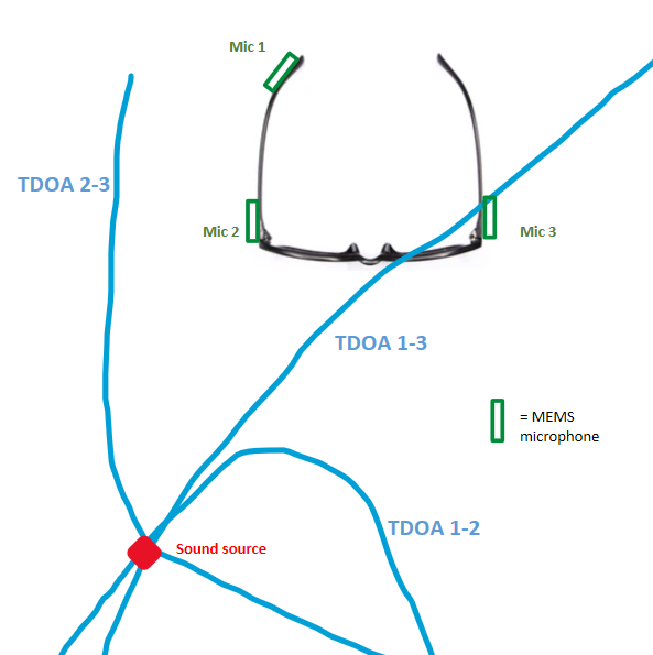
Figure 5: Diagram of microphone array
Instead of receiving a coordinate from this arrangement, we receive an angle of origin, and a distance to the origin, which can effectively be described as an arc on a plane through the origin (the user) and the origin of sound, with radius r, depicted in figure 6. This is where the camera helps out.
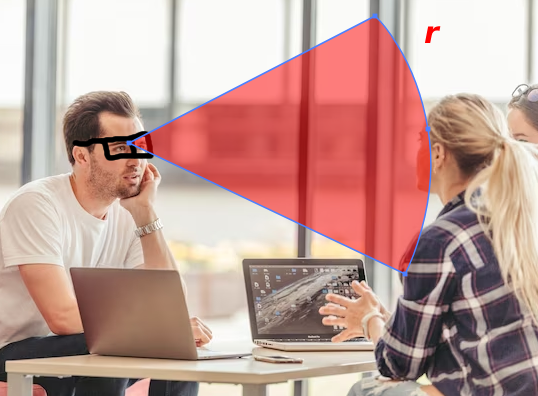
Figure 6: Visualization of what microphone array can tell us
Using an open-source computer vision system such as OpenCV, the device can recognize faces and more importantly, speakers in the field-of-vision of the user via facial positioning and movement in the mouth region. Given the information from the microphone array, the device knows what is being said, from which direction and approximately from how far. The camera gives the additional information of the elevation of the person speaking, how many speakers are in the conversation, and the orientation of the rest of the environment.

Figure 7: Example of OpenCV output
Using this information, it is possible for the device to display captions and other information in a much more detailed and embedded manner. The captions of a certain person can be displayed above or to the side of someone, as opposed to on predesignated locations on the smart glass display. These location based indicators allow for much more efficient communication of the location of a sound or speaker compared to any form of indicator through text.
The plan for the development of this device began with the Raspberry Pi platform, but we quickly realized we would need specialized hardware as well as extensive optimization in order to receive 4 simultaneous analog inputs along with a camera, and perform some heavy processing on all that data. Therefore we moved to development to a Linux machine. We are using 4 analog MEMS microphones, as these types of microphones are really the only ones suitable for our size needs. We put the output of the microphones through a bandpass filter with cutoff frequencies 90Hz-8kHz, as this range closely fits the frequencies required for speech-to-text algorithms. The output is then put through a single-rail op-amp in order to scale it to be a 0-5V signal. We use an ADC with I2C output to receive the analog inputs, and in order to get the data to the Linux machine we employ an I2C to USB bus. As for the facial detection aspect, our team decided to utilize OpenCV implemented in python to achieve accurate facial detection. From here OpenCV can be structured to detect and track small movements in the lower half of the facial region in order to predict when a user/users might be talking. All of this was compiled and coded in two corresponding python files for organization and for effentent development. All parts are linked below in the bill of materials. The Linux machine is used for development only, the platform for the final design is TBD.
4. Bill of Materials (BOM)
| Item # | Part | Manuf. | Description | Qty | Total Price | Link |
| 1 | CP2112 Breakout Board | Teyleten | I2C Bus Debug Board | 1 | 9.99 | CP2112 Breakout Board |
| 2 | ADS1015 Breakout Board | HiLetgo | 12-bit ADC Breakout Board | 1 | 8.99 | ADS1015 Breakout Board |
| 3 | TPS62122DRVR | TI | Buck Voltage Regulator | 2 | 2.46 | TPS62122DRVR |
| 4 | CMM-2718AT-38164W-TR | CUI | Analog MEMS Mic | 4 | 5.04 | CMM-2718AT-38164W-TR |
| 5 | OPA341NA/3K | TI | Single Input Op Amp | 4 | 11 | OPA341NA/3K |
| 6 | ERJ-2RKF3603X | Panasonic | 360kO SMD Resistor | 4 | 0.96 | ERJ-2RKF3603X |
| 7 | ERJ-2RKF2403X | Panasonic | 240kO SMD Resistor | 4 | 0.96 | ERJ-2RKF2403X |
| 8 | ERJ-2RKF1002X | Panasonic | 10kO SMD Resistor | 4 | 0.96 | ERJ-2RKF1002X |
| 9 | ERJ-2RKF1502X | Panasonic | 15kO SMD Resistor | 4 | 0.96 | ERJ-2RKF1502X |
| 10 | RN73R1ETTP1762F25 | KOA | 17.6kO SMD Resistor | 4 | 0.64 | RN73R1ETTP1762F25 |
| 11 | RMCF2512FT90R9 | Stackpole | 90.9Ω SMD Resistor | 4 | 0.60 | RMCF2512FT90R9 |
| 12 | GRM0335C1E150JA01D | Murata | 15pF SMD Capacitor | 4 | 0.44 | GRM0335C1E150JA01D |
| 13 | GJM0335C0J220JB01D | Murata | 22pF SMD Capacitor | 4 | 0.16 | GJM0335C0J220JB01D |
| Item # | Part | Manuf. | Description | Qty | Total Price | Link |
| 14 | T491A104K035AT | Kemet | 0.1uF SMD Capacitor | 12 | 4.08 | T491A104K035AT |
| 15 | TAJA475K016RNJ | KYOCERA | 4.7uF SMD Capacitor | 4 | 1.4 | TAJA475K016RNJ |
| 16 | MLZ2012M220WTD25 | TDK | 22uH SMD Inductor | 2 | 2.48 | MLZ2012M220WTD25 |
| 17 | BLM15AG102SN1D | Murata | FERRITE BEAD | 4 | 0.40 | BLM15AG102SN1D |
| 18 | PESD5V0F1BL,315 | Nexperia | TVS DIODE | 8 | 17.28 | PESD5V0F1BL,315 |
| 19 | Printed Circuit Board | Can vary | Main PCB | 1 | 24 | OSF | IRL Subtitles |
| 20 | 3D Printer Filament | Can vary | Glasses frame | 25 (g) | ~0.75 | OSF | IRL Subtitles |
| TOTAL | $93.55 | |||||
Tools Used
| Tool | Description | Price | Link |
| FreeCAD | Open-source CAD modeling software | Free | https://www.freecad.org/ |
| KiCAD | Open-source PCB design suite | Free | https://www.kicad.org/ |
| Ultimaker Cura | Open-source slicer | Free | https://ultimaker.com/software/ultimaker-cura/ |
| Ender 3* | Open-source 3D printer | $190 | https://www.creality.com/products/ender-3-3d-printer |
| Solder paste | These parts come in a variety of prices, qualities and quantities, or they may be found at a local makerspace | ||
| Solder oven** | |||
| Solder iron | |||
| Solder | |||
* any 3D PLA printer with a nozzle diameter <=4mm may be used
** a heat gun may be used as a replacement
6. Assembly Instructions
Disclaimer:
*When soldering be sure to utilize proper safety precautions like reviewing the safety data sheets for the solder that is being used, substitute lead-containing solder with lead-free solder, inspecting soldering gear for any damages before each use, solder away from flammable materials, use tweezers or clamps to hold wires or parts that are to be heated, use eye protection when soldering, use the soldering iron stand when the iron is not in use, and avoid any contact with the soldering iron. Avoid inhaling any fumes as some solder pastes may contain lead and tin. Excessive exposure to lead oxide fumes can result in lead poisoning.*
*When handling solder paste, avoid skin contact with solder paste such as the eyes, mouth, nose, or any sensitive areas. Wash hands thoroughly before and after use, maintain safe hygiene practices.*
*Refer to the MIT Soldering Safety and Health Guidelines for more information[9]*
Glasses Frame Replication:
The current frame is designed to fit the printed circuit boards in a press fit manner. This will not be the case for the final design, but it is sufficient for our testing purposes, and allows for flexibility which is also currently desired. The frames1.3.stl file can be found on the OSF repository, linked in the Bill of Materials, and the frames can be directly printed from there. We used the Ultimaker Cura software to slice the model into .gcode, and used PLA printed at 215O C for our model, but this can depend on your filament and printer. We used the print orientation shown in figure X and a support overhang angle of 75O to get rid of unnecessary support. The remaining supports are relatively easy to remove with a screwdriver, and then can be sanded down with sandpaper.
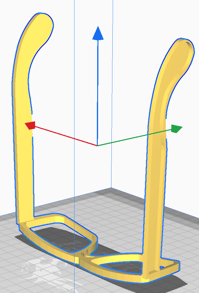
Figure 8: Screenshot from Ultimaker Cura
Also found at that link is the frames1.3.FCStd FreeCAD file. If you need to edit tolerances around the slot for the boards based on your printer’s performance, use this file. FreeCAD can be downloaded from the link provided in the Tools Used. In order to edit the slot for the PCBs, first open the part and expand the part hierarchy by clicking on the yellow part symbol shown in figure X.
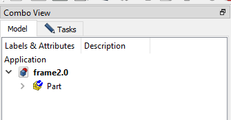
Figure 9: Screenshot of FreeCAD model/task window
Scroll down and select Sketch 003. The part may look like figure X now, making it hard to edit to pocket relative to the rest of the body.
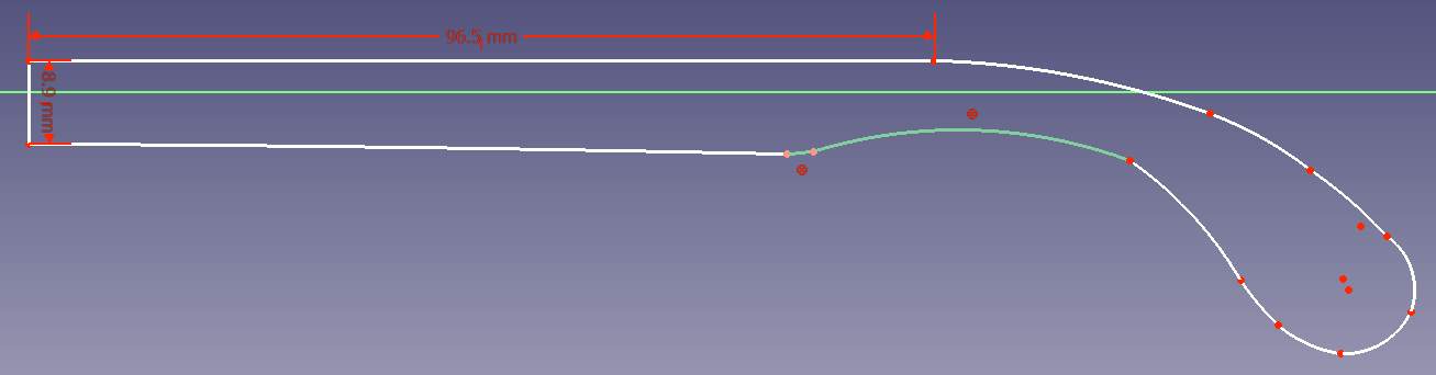
Figure 10: Screenshot from FreeCAD sketch of PCB pocket
To fix this, on the part hierarchy select Pad 001 and hit space. The rest of the part should show up, making it easier to edit the sketch. To edit the sketch, click and drag the necessary vertices in the sketch. Once you have made the proper edits, under the tasks tab, hit close.
Figure 11: Close a sketch in FreeCAD
Then, right click on the yellow part icon, and select Recompute Object to update the body. Then single click the yellow part icon to select the body, and go to File -> Export. There you can export the file to .stl format to be sliced in the Ultimaker Cura software.
Ordering the PCB:
Before the soldering construction of the PCBs can begin, the PCBs must first be obtained. The schematic and gerber files can be obtained on the OSF repository, linked in the Bill of Materials. There are multiple ways and places the PCB can be created or ordered from, this procedure instructs working through jlcpbc.com’s website.
To have the PCB’s printed, visit JLCPCB.com. On the website, click “Add gerber file” and select the zip file “memsArray_gbrs” within the memsBoard file, then click the “Instant Quote” button to move on. Once that has been completed, the page should look like the image below.
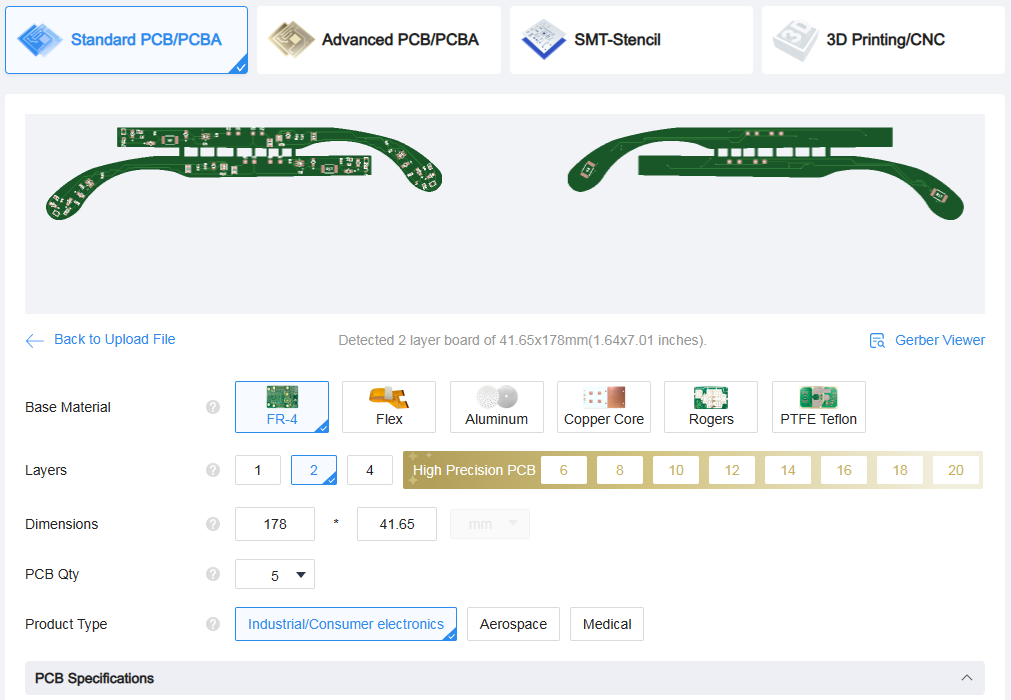
Figure 12: Instant Quote page
Ensure that the board settings look the same as the image above. The board will have two layers and a dimension of 178×41.65mm. Next up is the PCB Specifications. Ensure that the PCB Specifications are the same except for the PCB Color. The PCB Color option changes the color finish of the board and does not affect the operation of the board.
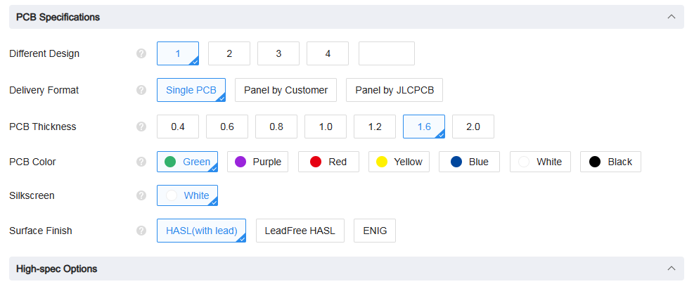
Figure 13: PCB Specifications
At the bottom of the page, there is an option to have the board assembled by JLCPCB. The following board assembly procedure instructs how to assemble the board. Finally click “Save to Cart” and the board is ready for purchase.
PCB Replication:
*The PCB was designed in KiCad 8.0 and it is highly recommended to have the “memsBoard.kicad_pcb” file open in KiCad while following along through the replication instructions.*
The procedure for assembling the PCBs will begin with the glasses left side (top) circuit board followed by the glasses right side (bottom) circuit board. Assume all components are to be placed on the front side of the circuit boards unless explicitly stated. The instructions utilize solder paste, a way of placing the components on the boards then baking the board in a reflow oven, however it is possible to solder the components onto the board by hand. Included below is an image of the PCB drawing.
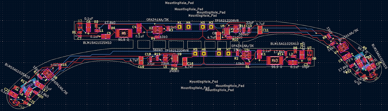
Figure 14: PCB drawing
- Begin by applying solder paste then placing the components to the solder pads for components C9, C12, C13, C14, D3, D4, L4, R12, U6. *It is recommended that R9 be soldered by hand on the second layer of the board (back side) after the front side components have been baked.* Refer to figure 15 for a close up image of the location of these parts. The values of the components is as follows:
| BOM Item # | P/N | Description | Schematic Item # |
| 4 | CMM-2718AT-38164W-TR | Analog MEMS Mic | U6 |
| 10 | RN73R1ETTP1762F25 | 17.6kO Resistor | R12, |
| 11 | RMCF2512FT90R9 | 90.9Ω Resistor | R9 |
| 12 | GRM0335C1E150JA01D | 15pF SMD Capacitor | C13 |
| 14 | T491A104K035AT | 0.1uF SMD Capacitor | C9, C12, C14 |
| 17 | BLM15AG102SN1D | FERRITE BEAD | L4 |
| 18 | PESD5V0F1BL,315 | TVS DIODE | D3, D4 |
Table 3: Parts for step 1
*Capacitors C9, C12, and C14 are polarized tantalum capacitors that require specific placement. Refer to the T491A104K035AT data sheet in the Bill of Materials for its polarization.*
*Diodes D3 and D4 require specific placement. Refer to the PESD5V0F1BL,315 data sheet in the Bill of Materials for its mounting specifications.*
*Microphone U6 requires specific placement. Refer to the CMM-2718AT-38164W-TR data sheet in the Bill of Materials for its mounting specifications.*
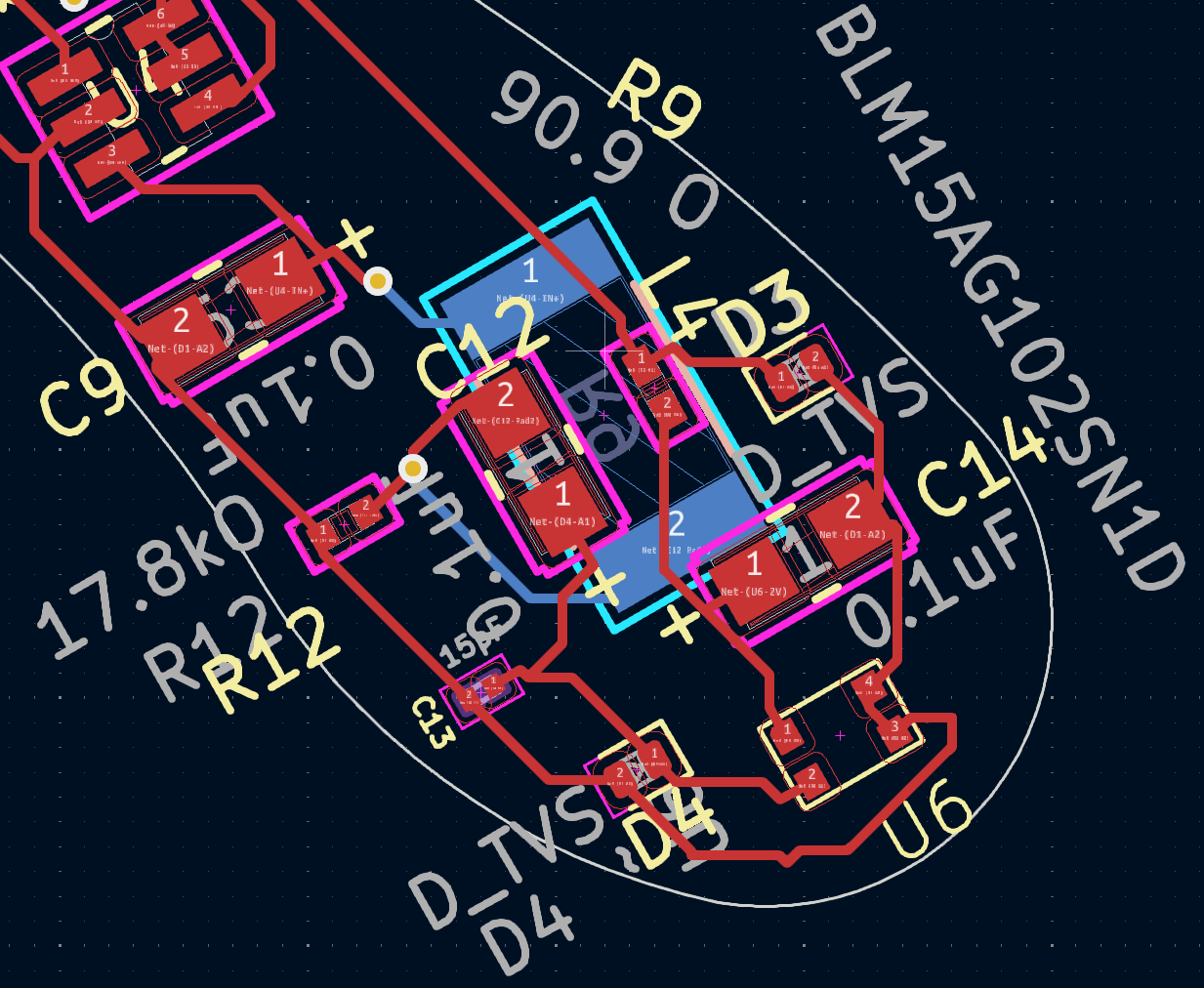
Figure 15: Top board temple Microphone region
- Just north of step one, apply solder paste and place components R7, R8, and U4. Refer to figure 16 for a close up image of the location of these parts. The values of the components is as follows:
| BOM Item # | P/N | Description | Schematic Item # |
| 5 | OPA341NA/3K | Single Input Op Amp | U4 |
| 8 | ERJ-2RKF1002X | 10kO SMD Resistor | R7 |
| 9 | ERJ-2RKF1502X | 15kO SMD Resistor | R8 |
Table 4: Parts for step 2
*Op-Amp U4 requires specific placement. Refer to the OPA341NA/3K data sheet in the Bill of Materials for its mounting specifications.*
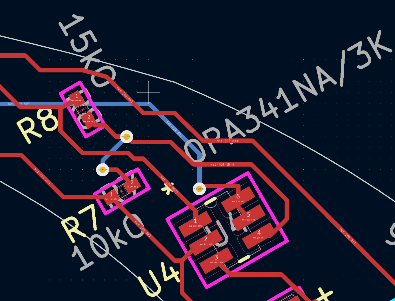
Figure 16: Top board temple Op-Amp region
- Next, apply solder paste and place components C8, U5, R10, L3, R11, C10, and C11. Refer to figure 17 for a close up image of the location of these parts. The values of the components is as follows:
| BOM Item # | P/N | Description | Schematic Item # |
| 3 | TPS62122DRVR | Buck Voltage Regulator | U5 |
| 6 | ERJ-2RKF3603X | 360kO SMD Resistor | R11 |
| 7 | ERJ-2RKF2403X | 240kO SMD Resistor | R10 |
| 13 | GJM0335C0J220JB01D | 22pF SMD | C10 |
| 15 | TAJA475K016RNJ | 4.7uF SMD Capacitor | C8,C11 |
| 16 | MLZ2012M220WTD25 | 22uH SMD Inductor | L3 |
Table 5: Parts for step 3
*The Voltage Buck Regulator, U5, requires specific placement. Refer to the TPS62122DRVR data sheet in the Bill of Materials for its mounting specifications.*
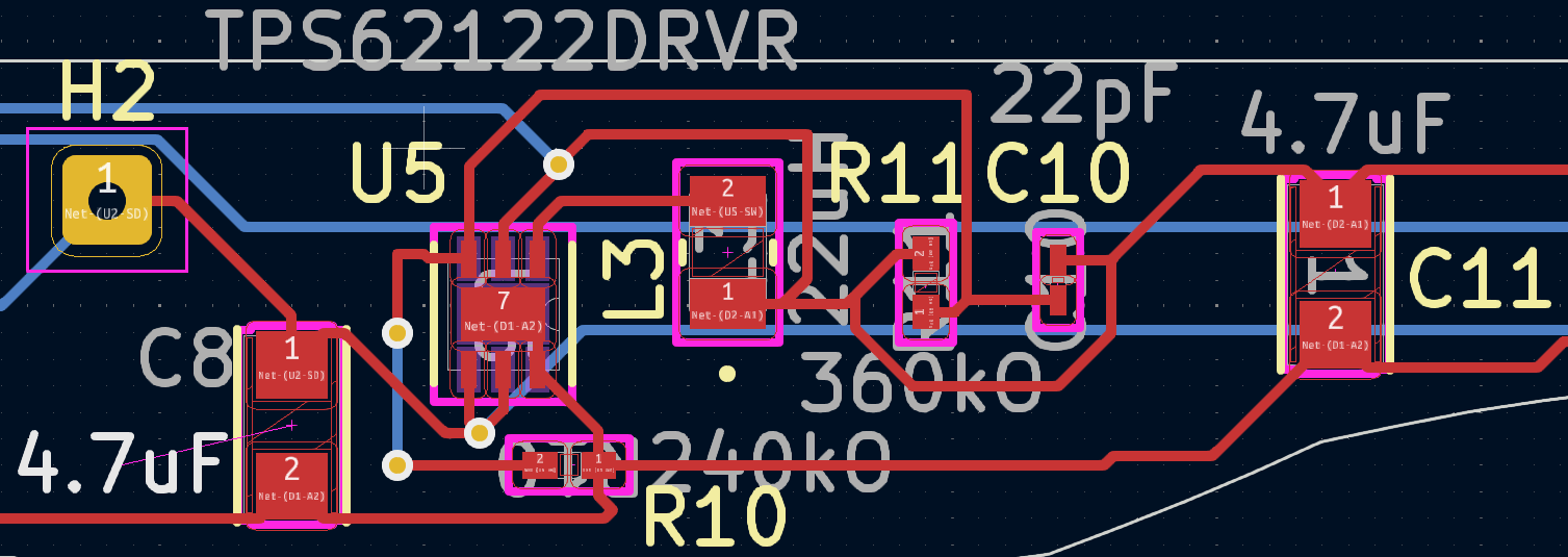
Figure 17: Top board mid arm
- Apply solder paste and place components C4, C5, C6, C7, D1, D2, L1, R3, R4, R5, R6, U3, U4. Refer to figure 18 for a close up image of the location of these parts. The values of the components is as follows:
| BOM Item # | P/N | Description | Schematic Item # |
| 4 | CMM-2718AT-38164W-TR | Analog MEMS Mic | U3 |
| 5 | OPA341NA/3K | Single Input Op Amp | U2 |
| 8 | ERJ-2RKF1002X | 10kO SMD Resistor | R4 |
| 9 | ERJ-2RKF1502X | 15kO SMD Resistor | R3 |
| 10 | RN73R1ETTP1762F25 | 17.6kO SMD Resistor | R6 |
| 11 | RMCF2512FT90R9 | 90.9Ω SMD Resistor | R5 |
| 12 | GRM0335C1E150JA01D | 15pF SMD Capacitor | C7 |
| 14 | T491A104K035AT | 0.1uF SMD Capacitor | C4, C5, C6, |
| 17 | BLM15AG102SN1D | FERRITE BEAD | L1 |
| 18 | PESD5V0F1BL,315 | TVS DIODE | D1, D2 |
Table 6: Parts for step 4
*Capacitors C4, C5, and C6 are polarized tantalum capacitors that require specific placement. Refer to the T491A104K035AT data sheet in the Bill of Materials for its polarization.*
*Microphone U3 requires specific placement. Refer to the CMM-2718AT-38164W-TR data sheet in the Bill of Materials for its mounting specifications.*
*Additional item comments on next page
*Diodes D1 and D2 require specific placement. Refer to the PESD5V0F1BL,315 data sheet in the Bill of Materials for its mounting specifications.*
*Op-Amp U2 requires specific placement. Refer to the OPA341NA/3K data sheet in the Bill of Materials for its mounting specifications.*
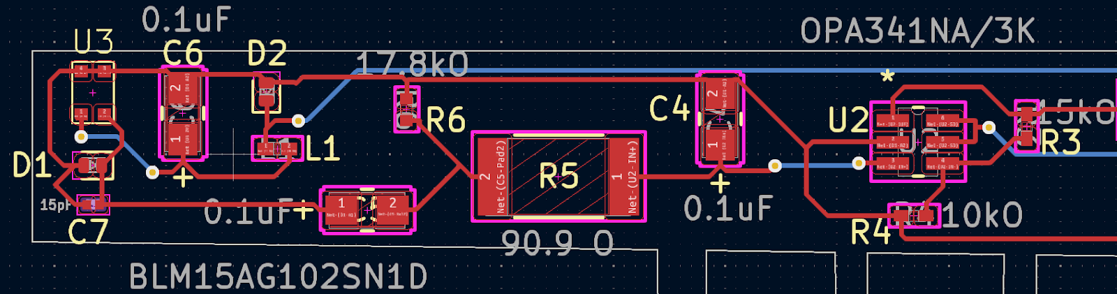
Figure 18: Top board front of arm
- Step 5 begins working on the placement of components on the glasses right side (bottom) circuit board. *It is recommended that R17 be soldered by hand on the second layer of the board (back side) after the front side components have been baked.* Apply solder paste and place components C17, C20, C21, C22, D7, D8, L6, R15, R16, R17, U8, U10. Refer to figure 19 for a close up image of the location of these parts. The values of the components is as follows with item comments after the table:
| BOM Item # | P/N | Description | Schematic Item # |
| 4 | CMM-2718AT-38164W-TR | Analog MEMS Mic | U10 |
| 5 | OPA341NA/3K | Single Input Op Amp | U8 |
| 8 | ERJ-2RKF1002X | 10kO SMD Resistor | R15 |
| 9 | ERJ-2RKF1502X | 15kO SMD Resistor | R16 |
| 11 | RMCF2512FT90R9 | 90.9Ω SMD Resistor | R17 |
| 12 | GRM0335C1E150JA01D | 15pF SMD Capacitor | C21 |
| 14 | T491A104K035AT | 0.1uF SMD Capacitor | C17, C20, C22 |
| 17 | BLM15AG102SN1D | FERRITE BEAD | L6 |
| 18 | PESD5V0F1BL,315 | TVS DIODE | D7, D8 |
Table 7: Parts for step 5
*Capacitors C17, C20, and C22 are polarized tantalum capacitors that require specific placement. Refer to the T491A104K035AT data sheet in the Bill of Materials for its polarization.*
*Diodes D7 and D8 require specific placement. Refer to the PESD5V0F1BL,315 data sheet in the Bill of Materials for its mounting specifications.*
*Op-Amp U8 requires specific placement. Refer to the OPA341NA/3K data sheet in the Bill of Materials for its mounting specifications.*
*Microphone U10 requires specific placement. Refer to the CMM-2718AT-38164W-TR data sheet in the Bill of Materials for its mounting specifications.*
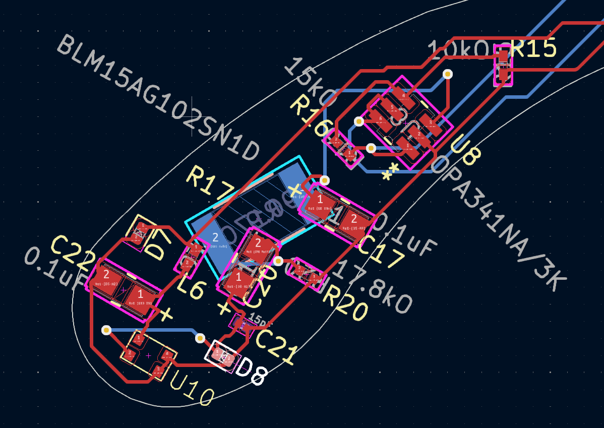
Figure 19: Bottom board temple region
- Apply solder paste and place components C16, C18, C19, L5, R18, R19, U9. Refer to figure 20 for a close up image of the location of these parts. The values of the components is as follows:
| BOM Item # | P/N | Description | Schematic Item # |
| 3 | TPS62122DRVR | Buck Voltage Regulator | U9 |
| 6 | ERJ-2RKF3603X | 360kO SMD Resistor | R19 |
| 7 | ERJ-2RKF2403X | 240kO SMD Resistor | R18 |
| 13 | GJM0335C0J220JB01D | 22pF SMD Capacitor | C18 |
| 15 | TAJA475K016RNJ | 4.7uF SMD Capacitor | C16, C19 |
| 16 | MLZ2012M220WTD25 | 22uH SMD Inductor | L5 |
Table 8: Parts for step 6
*The Voltage Buck Regulator, U9, requires specific placement. Refer to the TPS62122DRVR data sheet in the Bill of Materials for its mounting specifications.*
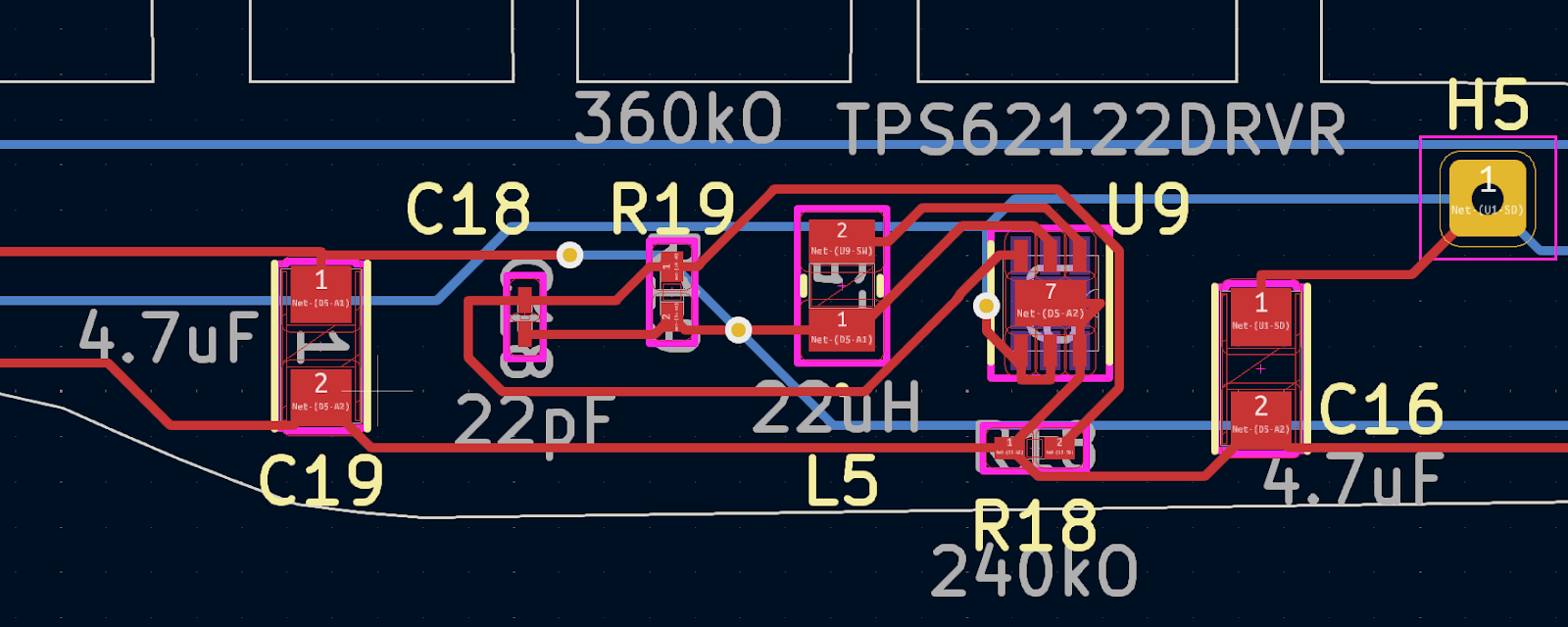
Figure 20: Bottom board mid arm
- Apply solder paste and place components R1, R2, U1. Refer to figure 21 for a close up image of the location of these parts. The values of the components is as follows:
| BOM Item # | P/N | Description | Schematic Item # |
| 5 | OPA341NA/3K | Single Input Op Amp | U1 |
| 8 | ERJ-2RKF1002X | 10kO SMD Resistor | R1 |
| 9 | ERJ-2RKF1502X | 15kO SMD Resistor | R2 |
Table 9: Parts for step 7
*Op-Amp U1 requires specific placement. Refer to the OPA341NA/3K data sheet in the Bill of Materials for its mounting specifications.*
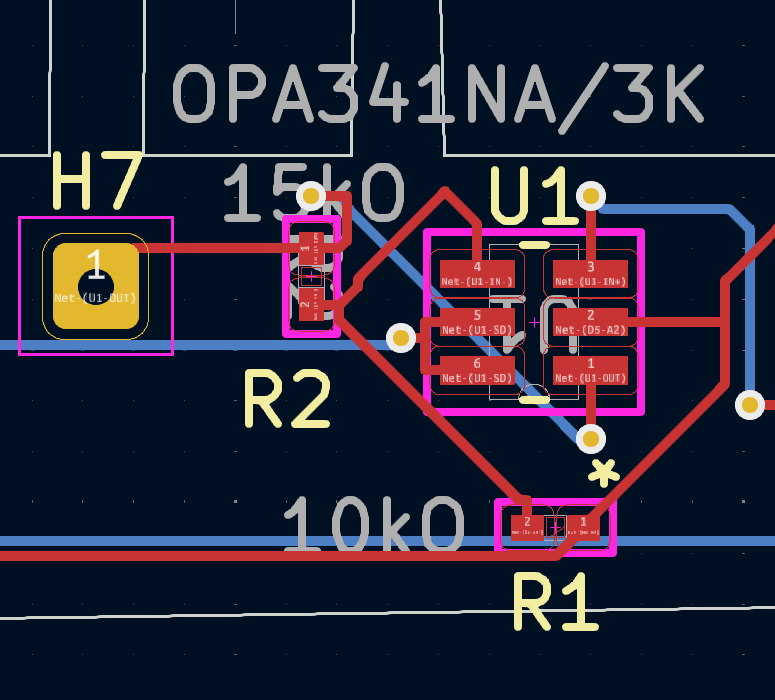
Figure 21: Bottom board front Op-Amp
- Apply solder paste and place components C1, C2, C3, C15, D5, D6, L2, R13, R14, U77. Refer to figure 22 for a close up image of the location of these parts. The values of the components is as follows:
| BOM Item # | P/N | Description | Schematic Item # |
| 4 | CMM-2718AT-38164W-TR | Analog MEMS Mic | U7 |
| 10 | RN73R1ETTP1762F25 | 17.6kO SMD Resistor | R14 |
| 11 | RMCF2512FT90R9 | 90.9Ω SMD Resistor | R13 |
| 12 | GRM0335C1E150JA01D | 15pF SMD Capacitor | C3 |
| 14 | T491A104K035AT | 0.1uF SMD Capacitor | C1, C2, C15 |
| 17 | BLM15AG102SN1D | FERRITE BEAD | L2 |
| 18 | PESD5V0F1BL,315 | TVS DIODE | D5, D6 |
Table 10: Parts for step 8
*Capacitors C1, C2, and C15 are polarized tantalum capacitors that require specific placement. Refer to the T491A104K035AT data sheet in the Bill of Materials for its polarization.*
*Diodes D5 and D6 require specific placement. Refer to the PESD5V0F1BL,315 data sheet in the Bill of Materials for its mounting specifications.*
*Microphone U7 requires specific placement. Refer to the CMM-2718AT-38164W-TR data sheet in the Bill of Materials for its mounting specifications.*
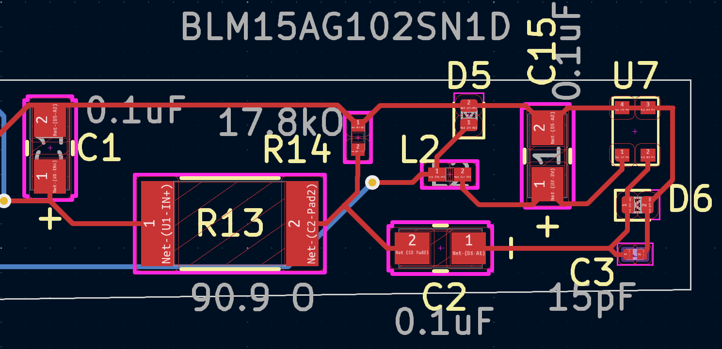
Figure 22: Bottom board front of arm
- Ensure that all components are accurately placed on top of the solder pads. Once all of the front side components have been placed on the boards using solder paste, the board is ready to be baked in a reflow oven. Once the boards have been baked, the 90.9kO resistors R9 and R17 are ready to be soldered onto the back of the boards. To solder these resistors onto the board by hand, it is recommended that flux, like Kester 951 flux, is used. Begin by turning on the soldering iron and an environmental fan. Once the soldering iron has heated up and is ready to be used, place a drop of flux onto the soldering pads of the board. Next, touch the soldering iron to the board’s pads to heat it and touch the solder wire to the soldering iron. Add a small amount of solder to the pad, a little goes a long way, then evenly coat the pad in solder. Repeat this process onto all four pads on the back of the circuit board.
Next place the 90.9kO resistor across the section so that the pads of the resistor align with the pads on the circuit board. Take the soldering iron and touch the connection of both the resistor and the circuit board pad to melt the solder and connect the resistor to the circuit board. Remove soldering iron from the pad so the solder can solidify. Repeat this process for all four pads on the back of the circuit board to connect the two 90.9kO resistors to the circuit board.
*It is highly recommended that once the board has been assembled that all components are tested for its value and conductivity using a multimeter.*
- If the printed circuit board does not come with through hole vias, which can be confirmed with a conductivity test, a wire will need to be soldered through the board to connect both sides of the board.
To do this, begin by finding a wire thin enough to fit through the via. The lead of a resistor or thin wire from a stranded wire works well. Then add a drop of flux to the solder pad on the side of the board that will be soldered. Touch the soldering iron to both the connection wire and the soldering pad. Add solder to the pad by touching a small amount of solder wire to the soldering iron. Add enough solder to cover the solder pad and to connect the connection wire to the pad. Remove the soldering iron to allow the connection to solidify and repeat on the opposite side of the board. Repeat this process for all vias on the circuit boards. For a simple guide on how to solder through surface items, refer to Figure 23[10].
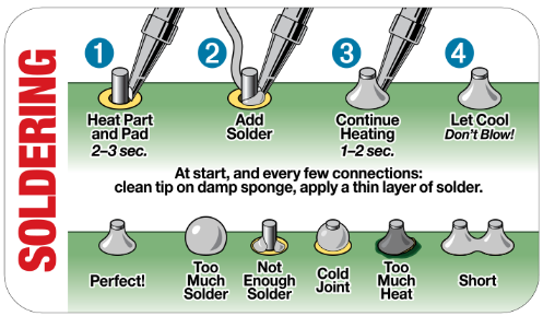
Figure 23: Soldering Reference Card [10]
- Sponsors/Acknowledgements
This project is currently self sponsored by the Open Source Hardware Enterprise.
- Sources
[1] “Sound localization,” Wikipedia, https://en.wikipedia.org/wiki/Sound_localization
[2]“How to Detect Speaker from facial landmarks of mouth using face_recognition – OpenCV Q&A Forum,” answers.opencv.org. https://answers.opencv.org/question/221780/how-to-detect-speaker-from-facial-landmarks-of-mouth-using-face_recognition/ (accessed Apr. 14, 2024).
[3]G. Gerganov, “whisper.cpp,” GitHub, Oct. 18, 2023. https://github.com/ggerganov/whisper.cpp
[4]K. Hendrikse, “TDOA Sound Localization with the Raspberry Pi,” Medium, Dec. 17, 2023. https://medium.com/@kim_94237/tdoa-sound-localization-with-the-raspberry-pi-3e777469c4fa#:~:text=TDOA%20sound%20localization%20requires%20the
[5]xrai.glass. https://xrai.glass/
[6]“Object Tracking Using Time Difference of Arrival (TDOA) – MATLAB & Simulink,” www.mathworks.com. https://www.mathworks.com/help/fusion/ug/object-tracking-using-time-difference-of-arrival.html
[7]A. Kafaei, Bahador Makkiabadi, A. Pourmohammad, and Seyed Hani Hozhabr, “Sound Source Localization Using Time Differences of Arrival; Euclidean Distance Matrices Based Approach,” Dec. 2018, doi: https://doi.org/10.1109/istel.2018.8661037.
[8]Z. El Chami, A. Guerin, A. Pham and C. Servière, “A phase-based dual microphone method to count and locate audio sources in reverberant rooms,” 2009 IEEE Workshop on Applications of Signal Processing to Audio and Acoustics, New Paltz, NY, USA, 2009, pp. 209-212, doi: 10.1109/ASPAA.2009.5346501.
[9]“New reference card: Soldering 101,” Adafruit Industries – Makers, hackers, artists, designers and engineers!, https://blog.adafruit.com/2016/12/26/new-reference-card-soldering-101/
[10] “EHS-0167 Soldering Safety and Health Guidelines,” MIT EHS Soldering pdf, https://ehs.mit.edu/wp-content/uploads/EHS-0167.pdf