
Week of September 11:
- Researched ATX Power Supply DC-DC conversion methods
- Researched Buck converter options
- Familarized with SPICE simulations
Week of September 18:
- Researched appropriate power factor for U.S. mains simulation
- Researced options for IC controller for DC/DC conversions
Week of October 1:
- Researched options for stepping down high voltage DC to usable DC
- Researched options for LLC DC step down converter
- Analyzed capacitance and inductance values on a physical power supply
Week of October 22:
- Researched design considerations for DC-DC Buck Converters
- Begin calculating component values for Buck Converters
- researched options for 12 V inversion IC
Week of October 30:
- Aquired test computer system for future power supply testing
- Researched TI Buck controller IC options
Week of January 21:
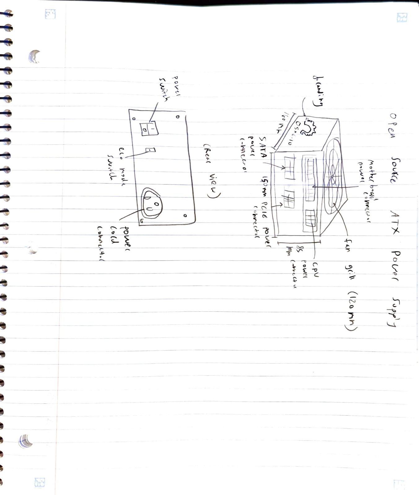
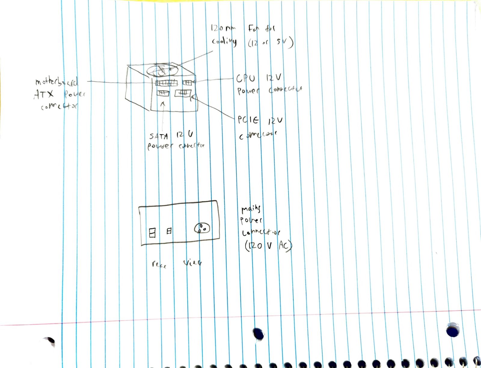
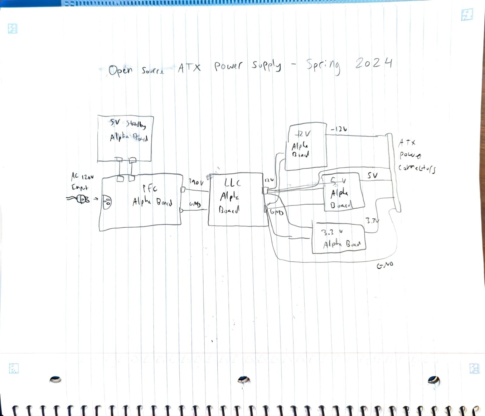
- Sketch of final ATX Power Supply design
Next week tasks:
- Finalize IC choice for 3.3 V Buck converter
- Finalize IC choice for 5 V Buck converterv
- Investigate options for 12 to -12 V converstion topology
Week of January 28:
- Narrowed down IC choice for 3.3 V and 5 V buck converter
- Chose IC from narrowed down options
- Researched options for using buck converter for -12 V conversion
Next Week’s Tasks:
- Begin schematic design for 5 V buck
- Choose buck converter for -12 V conversion
Week of February 4:
- Learned how to load schematics into KiCad for 5 V buck converter
- Researched requirments for -12 V buck converter
Next Week:
- Finish Schematic loading for 5V buck converter
- choose IC for -12 V buck converter
Week of February 11:
- Schematic Design for 5V buck converter
- Load Schematic for 3.3 V buck converter into KiCad
Next Week:
- Finish Schematic Loading for 3.3 V Buck Converter
- Finish Schematic design for 5 V buck converter
Week of February 18:
Project Progress:
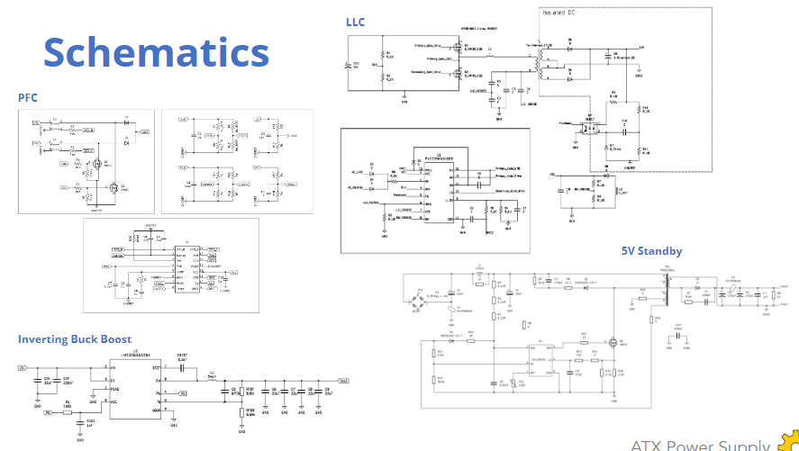
- Reviewed schematic for 5 V DC/DC Buck converter
- Reviewed schematic for 3.3 V DC/DC Buck converter
Next Week:
- component selection for 5 V DC/DC breakout
Week of March 3:
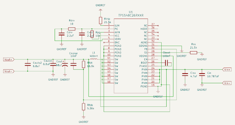
- Finished KiCad Schematic for 5 V DC/DC conversion
- New selection for 5 V buck converter chip
Next Week:
- New selection for 3.3 V buck converter chip
- Finish KiCad schematic for 3.3 V DC/DC conversion
Week of March 10:
- Finished KiCad Schematic of 3.3 V DC/DC conversion
- completed schematic review documents for 5 V and 3.3 V circuits
Next Week:
- BOM creation for 5 V components
- BOM creation for 3.3 V components
Week of March 17:
- Footprint importing for 5 V schematic
- Footprint important for 3.3 V schematic
Next Week:
- PCB layout finished for 5 V schematic
- PCB layout finished for 3.3 V schematic
Week of March 24:
- PCB general component layout for 3.3 V alpha board
- PCB trace routing begun for 3.3 V alpha board
Sketch of current design for end of Spring 2024 Semester:
- The design has changed considerably from the original as we are now not going to be making the first prototype in the ATX form factor but rather in individual alpha PCBs of each subsystem to make integration and testing less formidable. Each board will be connected to the next board in the conversion process via terminals and there will be several test points to test functionality once assembly is complete.
Next Week:
- PCB layout for 5V board complete
- Order components from BOM for 3.3 V and 5 V boards
Week of March 31:
- Worked on trace placement for 3.3 V PCB
- Worked on general component layout of 5 V PCB
Next Week:
- Begin compiling documentation for 5 V and 3.3 V conversion circuits for final report
- Begin comiling documentation for planned testing suite for hardware once assembled
Week of April 7:
- Worked on documentation for methodolgy and characterization of 5 and 3.3 V converters
- Worked on documentation for the planned tests that will be conducted on the boards once assembled
Next Week:
- Complete PCB layouts for 5 and 3.3 V PCBs complete
- Finish documentation for 5 and 3.3 V converters for final report
- Finalize project check off demonstration procedures
Week of April 14:
- Finished Documentation for 5 and 3.3 V converters for final report
- Prepare for project spec rundown on Tuesday
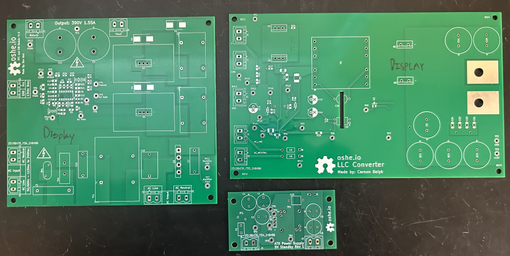
- Image of completed AC/DC boards:
Next Week:
- Any further preperations for project spec rundown before Tuesday
- Project spec rundown on Tuesday