
ATX Power Supply Spring 2024
1/21/24 – 1/27/24
MOSFET Selection
- MOSFET’s are a key component of both the PFC and LCC switching converters systems being used.
- Ensuring the MOSFETs meet that voltage and current ratings need of them is crucial to prevent overheating
Looking at the needed requirements:
- IDpeak = [PFC: 26.6A, LLC: 7A]
- ID = [PFC: 4.69A, LLC: 4.7A]
- TONmax = [PFC: 10.3uS, LLC: 16uS]
- VDSmax = [PFC: 500V, LCC: 600V]
To reduce cost we want to identify a MOSFET that both the PFC and LLC can use. This resulted in minimum requirements of IDpeak > 26.6A, ID > 4.7A, TONmax > 10.3uS, VDSmax = 600V
Using these parameters a MOSFET was selected that meets the SOP: IRFB9N60A
1/28/24 – 2/3/24
Custom Coupled Inductor
- Required for PFC is a coupled inductor used for sensing the zero crossing point
- Because of the specific turns ration needed, a custom wound inductor is needed
Design Considerations
- When design a coupled toroid inductor, one of the driving design consideration is physical size. However also ensuring the inductor does not saturate is necessary for proper operation
- When selecting a toroid core, selecting the an appropriate AL is crucial to ensuring that there is an appropriate about of primary and secondary turns need for a the need Inductance on the primary, 100uH, and a 5mA output from the secondary
2/4/24 – 2/10/24
Continuing the work from last week, a magnetic core and its primary and secondary winding wires are need for power factor correction inductors
Core Considerations
- The core needed must not saturate under maximum conditions. Core material properties and size play a role in this.
- The number of turns needed to meet the specified inductance along with the secondary turns can fit in the core window
2/11/24 – 2/17/24
Finalizing the magnetic core selection and winding wire calculations a core was selected to be used for converting the UCC28064A Evaluation Module to the UCC28065 IC which will be used in our final design.
Moving forward, passive components need to be selected and identified for the the UCC28065 moving towards the goal of a first revision of boards
2/25/24 – 3/2/24
Spring Break
3/3/24 – 3/9/24
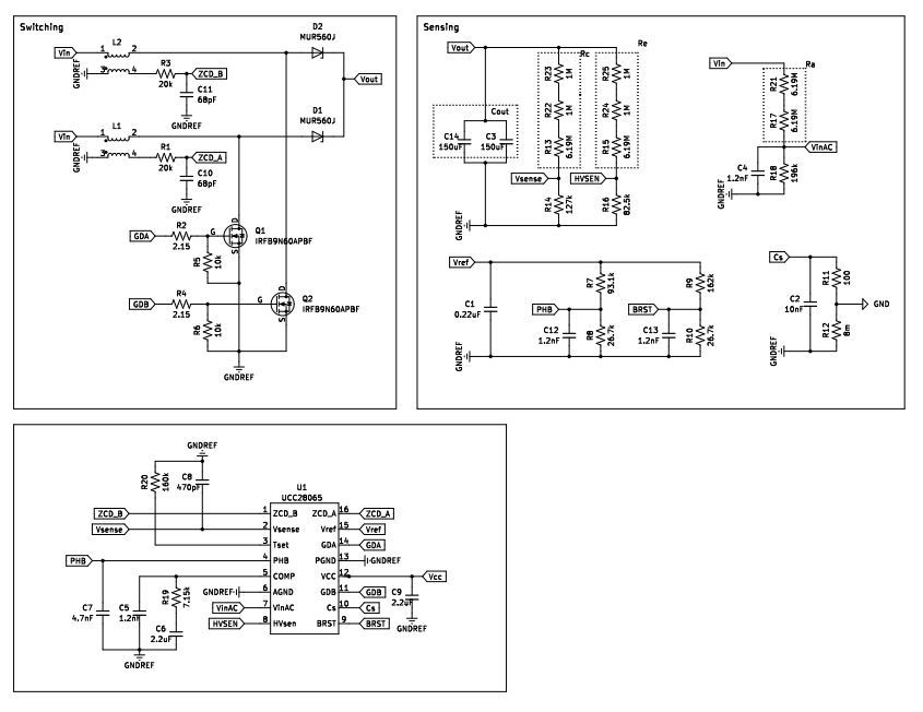
Began working on passive selection for the PFC schematic, with the goal of keeping SMD components larger then 0603 package size to keep.
Determined wattage and voltage ratings for resistors and capacitors used.
3/10/24 – 3/16/24
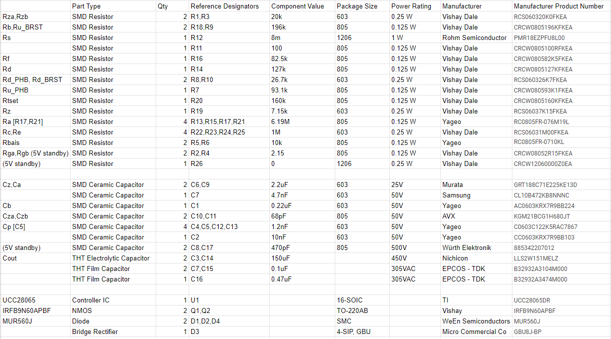
Finished the rest of the passive selection and importing all the proper data into the Kicad schematic file
Began working on creating documentation for a schematic review with our project sponsor. Moving forward we will look to begin layout for our first revision of test boards.
3/17/24 – 3/23/24
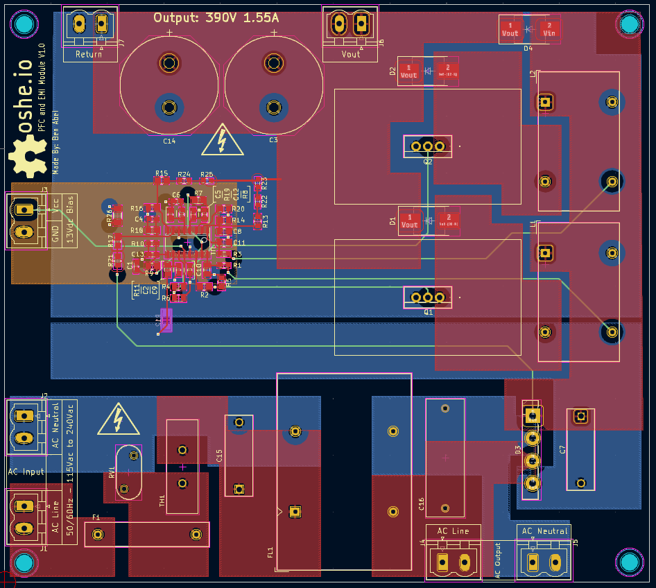
Beginning layout design, the goal with the first revision of boards is to produce a physical implementation of the schematic designs that we have been working on. While EMI compliances is an important aspect of board design, for our first revision we are more concerned with producing a board with will simply meet the given specification for it.
For the PFC and EMI board which I am working on, the main objective is to take a 50/60Hz 115Vrms to 240Vrms input wall voltage and output 390Vdc at 1.55A, which roughly equates to the 600W output goal. this output voltage then feeds into the LLC Module where it will be stepped down to and isolated 12 volts.
3/24/24 – 3/30/24
Finishing up the board layout, as seen below,
3/31/24 – 4/6/24
This week we aimed to finalize and order our boards for each respective subsystem as well as finalizing our BOMs for parts order. After reviewing assembly options through JLCPCB, it was determined that cost wise and knowledge wise we would be better off populating the boards ourselves. This gives us the added benefit of providing instructions for any at homer replicated this product to use similar reflow temperatures that we aim to use if they are unfamiliar with the process. As seen below for the EMI and PFC board, that I have been working on, the BOM was finalized and setup to allow Digikey’s list functionality to be used for easy parts ordering.
After reviewing the PCB layout with our sponsor, and making the recommended changes and additions to our respective boards, the Gerber files were generated utilizing a standard board thickness of 1.6mm and 2oz outer lay copper to help handle the peak current that will be seen.
4/7/24 – 4/13/24
This week while we waited on our components and PCBs to be shipped, we began working on finalizing the education material for our respective subsections. Building off the schematic review document that which was made earlier in the month, the goal of the education documentation for the PFC and EMI is for someone trying to replicate this design to understand the design decision that were made. This involves explaining how and why certain components were selected to be certain values and what that means for setting system parameters for how the PFC operates.
Moving forward as we get parts in, we will begin build and populating the boards to hopefully run some rudimentary test to ensure basic functionality
4/14/24 – 4/20/24
At the beginning of this week our board finally arrived along with their accompanying stencils. Ideally we wanted to build and test these boards, but with the constrains of finals week, as well as design expo, we decide it best to wait as we realistically wouldn’t have the time to their functionality. In leu of not populating the boards, we decide to more heavily focus on the documentation side of thing.
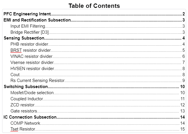
The goal with the documentation for the revision 1 boards is to provide a framework of the design choices and considerations for our respective boards. For my case with the EMI and PFC board, I looked to explain most all of my component choices, what there values where, why they where pick, why there ratings where selected to be what they where and so forth. The listed table of Contents below roughly outlines all the aspects of the schematic which were covered.
9/06/24 – 9/13/24
Coming back from the break with the PFC and LCC boards in hand, as well as a majority of the components need, we began building up our boards and winding the transformers. That process took up a majority of weeks 1 and 2. Last week after getting the board fully build, I ran the first power up and everything worked as expected under no load, with the PFC chip turn on at the 85Vrms as specified and outputs the correct voltage. Moving forward from here over the next 2 weeks I will be looking to finish up all the testing that I need to ensure my design is working properly, then move on to design the PCB for the finial build under the form factor constraints.
9/14/24 – 9/20/24
After getting the LLC transformer wound, it was determined that new capacitors would be needed for the resonant circuit and because of this most of this week was waiting on parts. While we waited we began testing on the 5V standby circuit, fully populating the board, and powering it up. Unfortunately, it didn’t operated properly and in the attempted trouble shooting process the MOSFET blew. Our plan moving forward with the 5V standby circuit is to populate a new board and test functionality from there. Moving forward into next week, we hope to set up a date to load test of both the LLC and PFC boards and began combining the schematics.
9/21/24 – 9/27/24
This week involved testing and debugging of the 5V standby circuit and the LLC Board as well as beginning the schematic combination of the PFC and LLC Boards. Firstly after populating the 5V standby board we where unable to get it output its proper 5Vs and during the debugging efforts the Mosfet and IC where destroyed. Because its functionality is not super critical to our design we decided to shift focus to continuing the debugging efforts on the LLC transformer.
With the new resonate capacitors in and replace on the LLC board we began to see better results on the output, but they were still no where near the target voltage. After diving deeper it was found that there were multiple resistors with the wrong values and a diode placed in the wrong position in relation to a sensing resistor divider network. After correcting this, we where seeing better results but there is still an issue with the RVCC voltage not being 13 volts.
Moving forward into CDR week, we have shifted focus to beginning the schematic capture combination and next week we hope to continue and find the remaining issues with the LLC Board.