
Background
The goal of this project is to create an Open-Source 600W computer power supply that meets commercial power supply standards. In our initial research for this project, we were unable to find any open-source computer power supplies or even similar higher-current power supplies. Our power supply will be relatively easy to build, and our goal is to have a BOM that’s 20% cheaper than similar commercially available power supplies. In addition, through this project, we will contribute a functional power supply design that’s capable of relatively high current output to the open-source community.
Structure
The project was started through a team review of the main architecture present in an ATX power supply. This review was aided by the Intel ATX Design Guide. We made a high-level flow diagram to visualize each power system and the requirements of an ATX power supply.
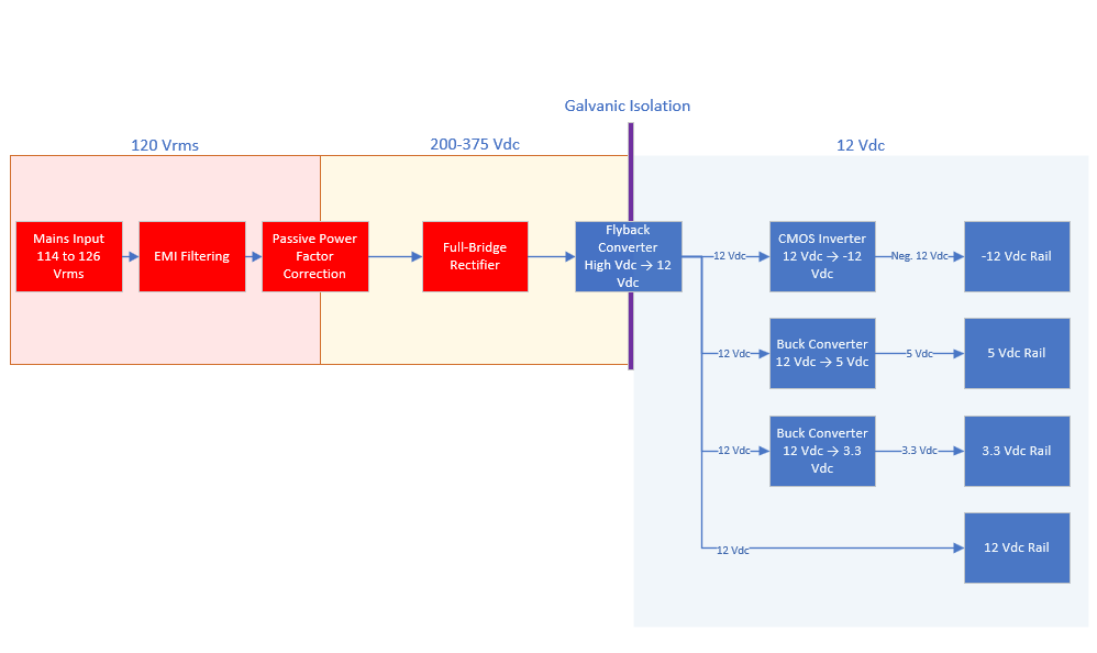
This breakdown of the main architecture made it easy to divide our team into specific fields which included AC-DC, DC-DC, and Case design.
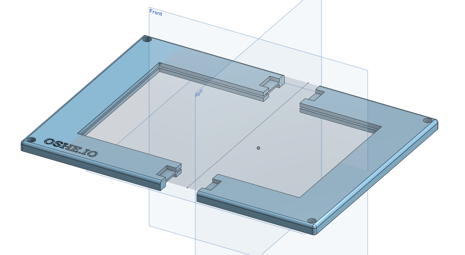
Case Design
- First Iteration
- Case size: (150 x 86 x 160 mm)
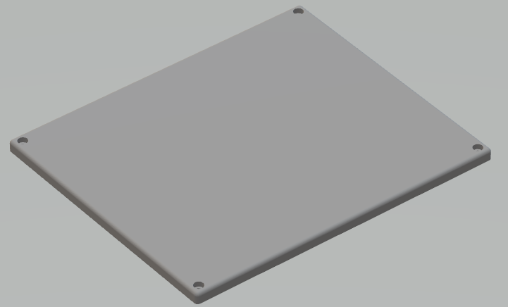
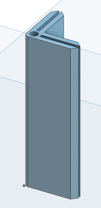
- The first iteration of the case design features 4 slots which are designed to take 16-gauge aluminum sheet metal. The bottom side of the case features an opening for a 120 mm computer fan used for cooling.
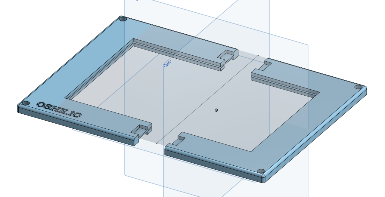
- Second Iteration
- After the first iteration design, ran into issues with the lab 3-D printers not being able to handle the print size and print time. This iteration focuses on making the print more modular and easier to print by moving away from the large print structures. The top and bottom of the case are made from the two structures on the right, this structure allows aluminum sheet metal to be inserted and pressed together. Super glue and 3-D printed tabs are then added to adhere the two structures together. After more testing with this iteration, the print quality on the OSHE lab printers did not improve and the lab 3-D printers were still malfunctioning.
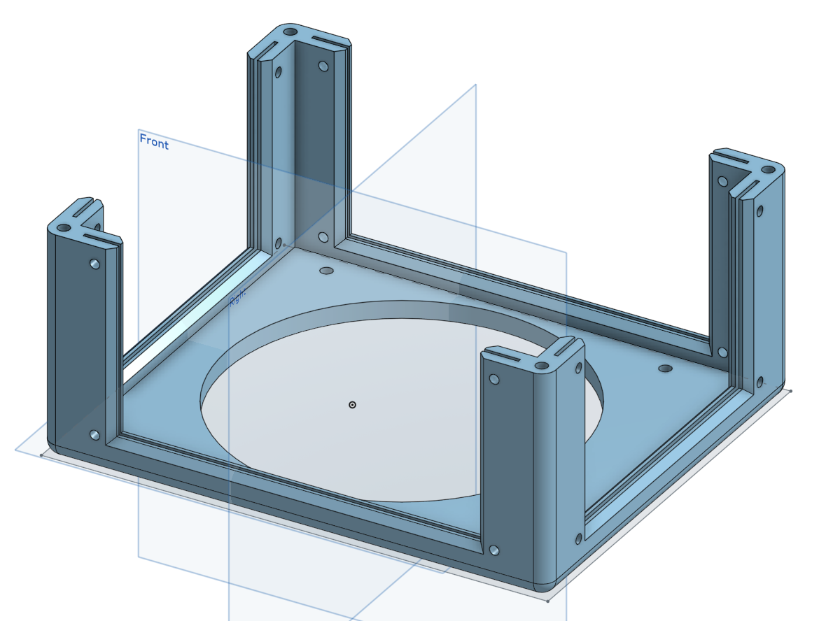
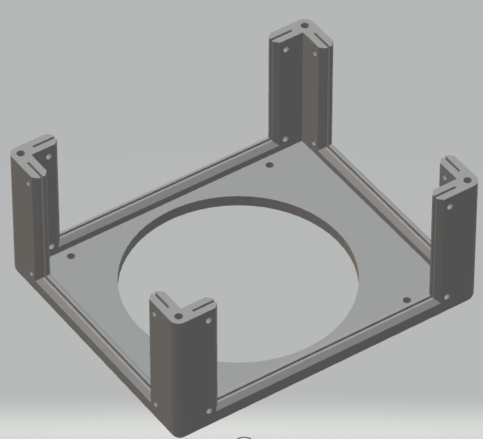
- Third Iteration
- To keep more structural integrity on the bottom side of the case (where the fan attaches) and due to the modular design not helping the print quality, the third iteration took the more stable base of the first iteration and the modular top of the second iteration to allow more surface area of metal to help with radiated emissions. In future iterations, we are planning to use copper tape to help with radiated emissions due to the entire case not being made of metal and is not able to act as a Faraday cage.
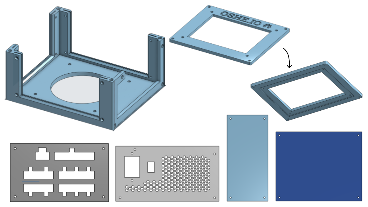
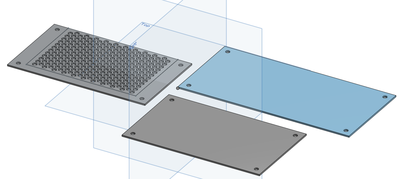
- Fourth Iteration
- This case iteration can bolt onto an ATX PC case by using the 4 screw holes showcased on the vent stencil (2nd from the left). These 4 3-D printable stencils will be helpful when cutting out the aluminum sheet metal to fit airholes, peripheral, CPU, SATA, and power connectors. After a 3-D print of the top lid failed, we moved to a recessed area where the 16-gauge sheet metal can be screwed down into the 3-D printed lid.
Power Factor Correction (PFC)
An important aspect of most all power supplies is PFC or power factor correction. Power factor correction is a useful technique used to help improve efficiency, reduce harmonics and lower the input current draw requirements. When looking at PFC, there are two methods which can be used: Active or Passive. Passive PFC consists of passive components, mainly inductor and capacitor, in a variety of different topologies, to remove any unwanted harmonics and improve power factor. However, passive PFC is mainly aimed at low power applications, as with high powers, larger components are needed. Active PFC works through the use of switching, typically in a boost converter configuration. While it offers the same capabilities of passive PFC, the main benefit to active is its dynamic ability.
After determining that we wanted to use active PFC, an IC was selected, the UCC28065 from Texas Instruments. This IC uses 2 boost converters in parallel, which provides the benefit of smaller component sizing, due to the smaller currents that are seen in each converter configuration. Another important aspect of the UCC28065 is its variability in input voltages and frequencies. Because of this the power supply can take in both North American mains, but as well as European mains. As shown below in the table, the design specs for the UCC28065 can be seen, as well as the schematic.
| Design Specs | ||
| Input Voltage [RMS] | Min | 85 Vrms |
| Max | 265 Vrms | |
| Input Frequency [Hz] | Min | 47 Hz |
| Max | 63 Hz | |
| Maximum Output Power | 600W | |
| Full load Efficiency | 90% | |
| Power Factor Correction Level | 0.98 | |
| Minimum Switching Frequency | 50 kHz | |
| Output Voltage | 400 V | |
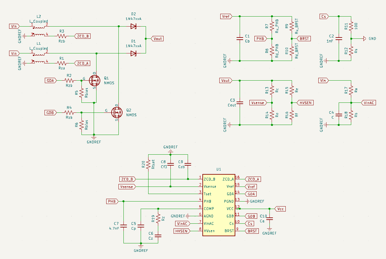
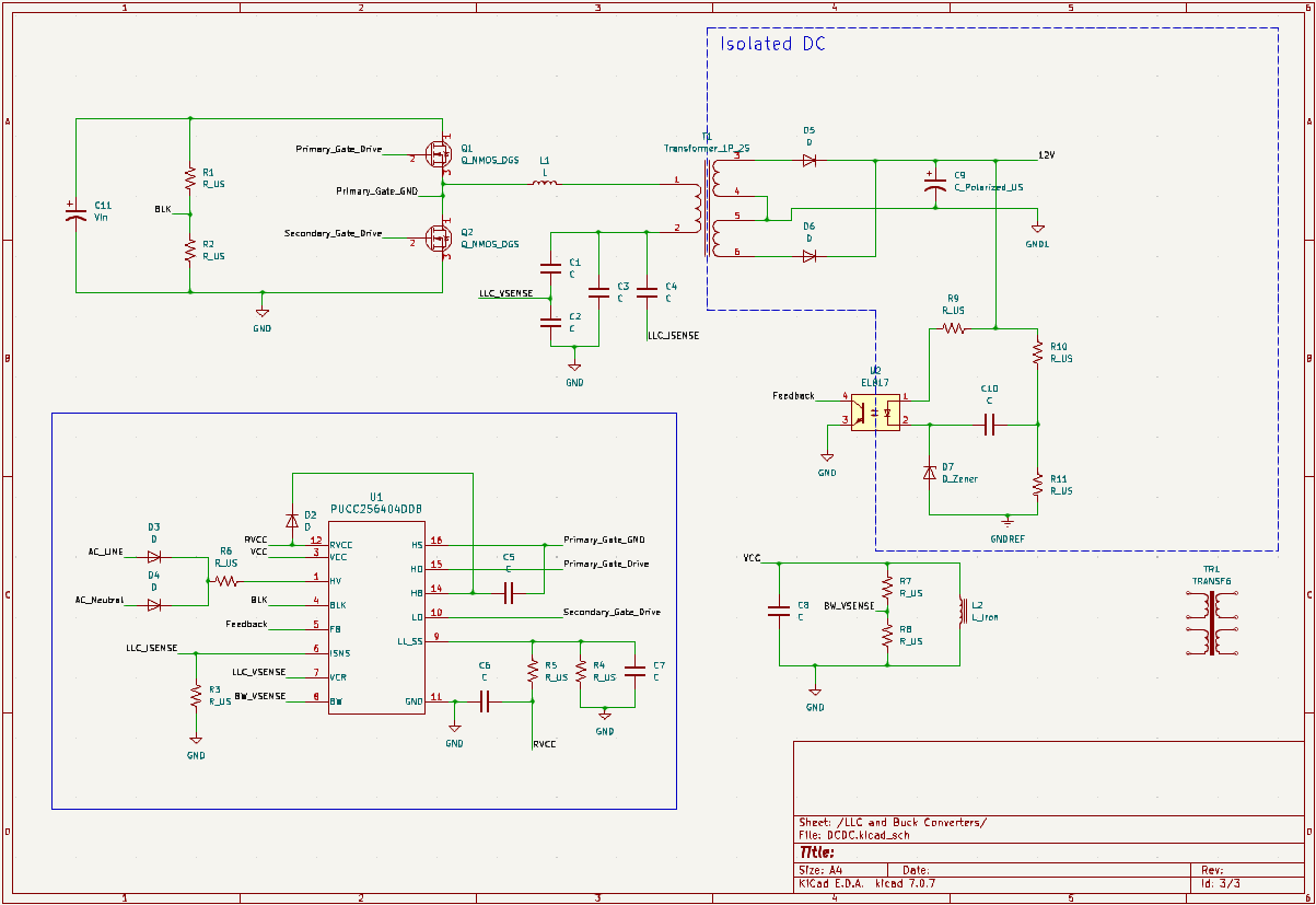
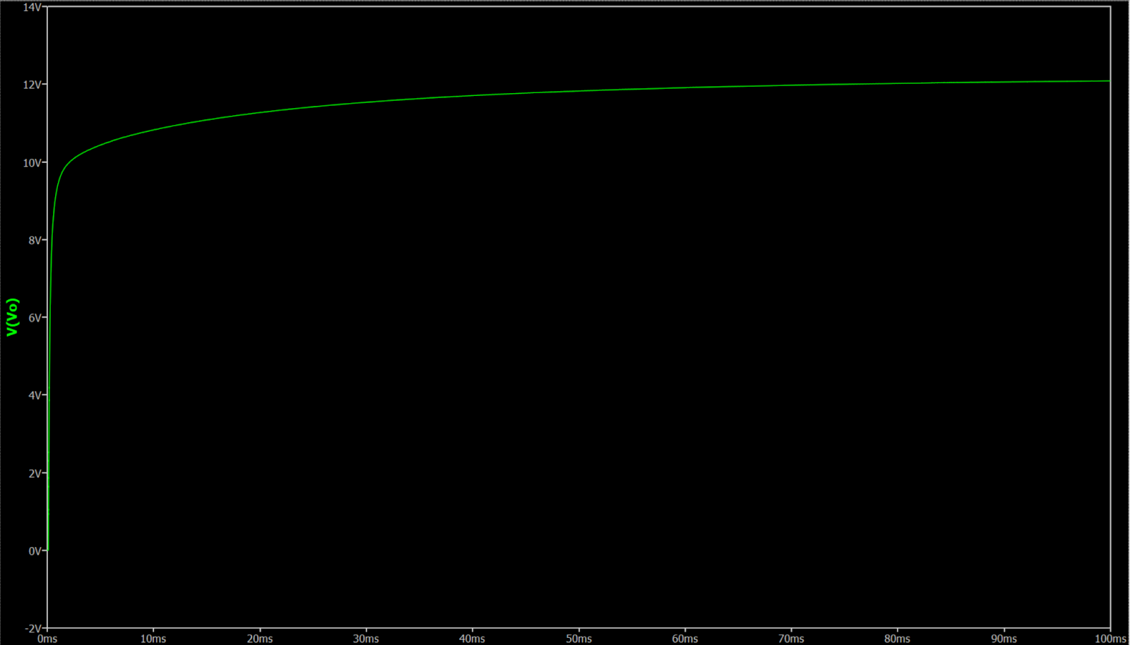
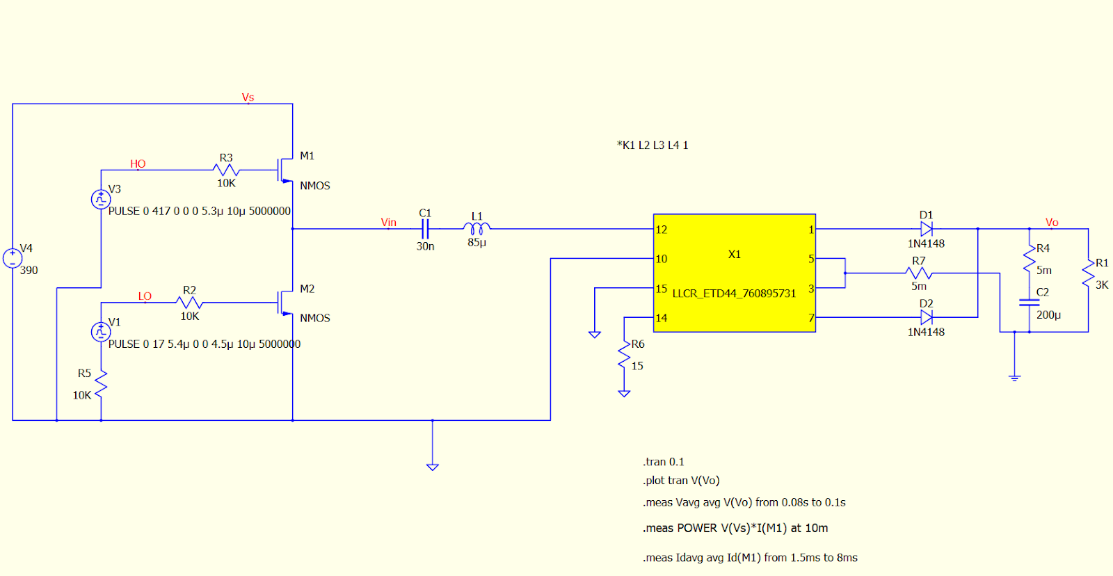
LLC Converter and Simulations
Since the PFC block outputs ~390V, a converter is required to step the voltage down to 12V for our secondary side while isolating both parts of the PCB from each other. One style being considered was a Flyback converter as it provides both isolation and large conversion ratios between the input and output side. During our research into Flyback converters, we found the LLC converter topology which has the same two benefits as the Flyback converter. The main benefit of using an LLC topology over Flyback is their very high efficiency at high power levels. The leakage inductance created by the transformer can be used as part of the resonant inductor, eliminating efficiency losses in the system. Below is the schematic for the LLC Converter topology with the included IC.
Simulations
After deciding to use an LLC converter to step down the voltage from the output of the PFC, we needed to select an IC and magnetics. We decided to go with TI’s UCC25640x family of LLC controllers because they are designed to pair with the PFC controller we have selected and it has integrated MOSFET drivers so a separate gate driver isn’t required. Next I worked on making some simulations to verify resonant component choices without destructive testing. The simulation is working with an ideal pulse waveform generated by the software but is having issues with driving MOSFETs to produce the output. One of the drawbacks in our simulation is the lack of feedback control so the load shown will not actually pull 600W but instead is set so the output is at 12V in the simulation waveform. The overall goal was to verify the choice of passive for the resonant circuit, not the total power output due to the complexities of adding closed-loop feedback control to a simulation within QSPICE.
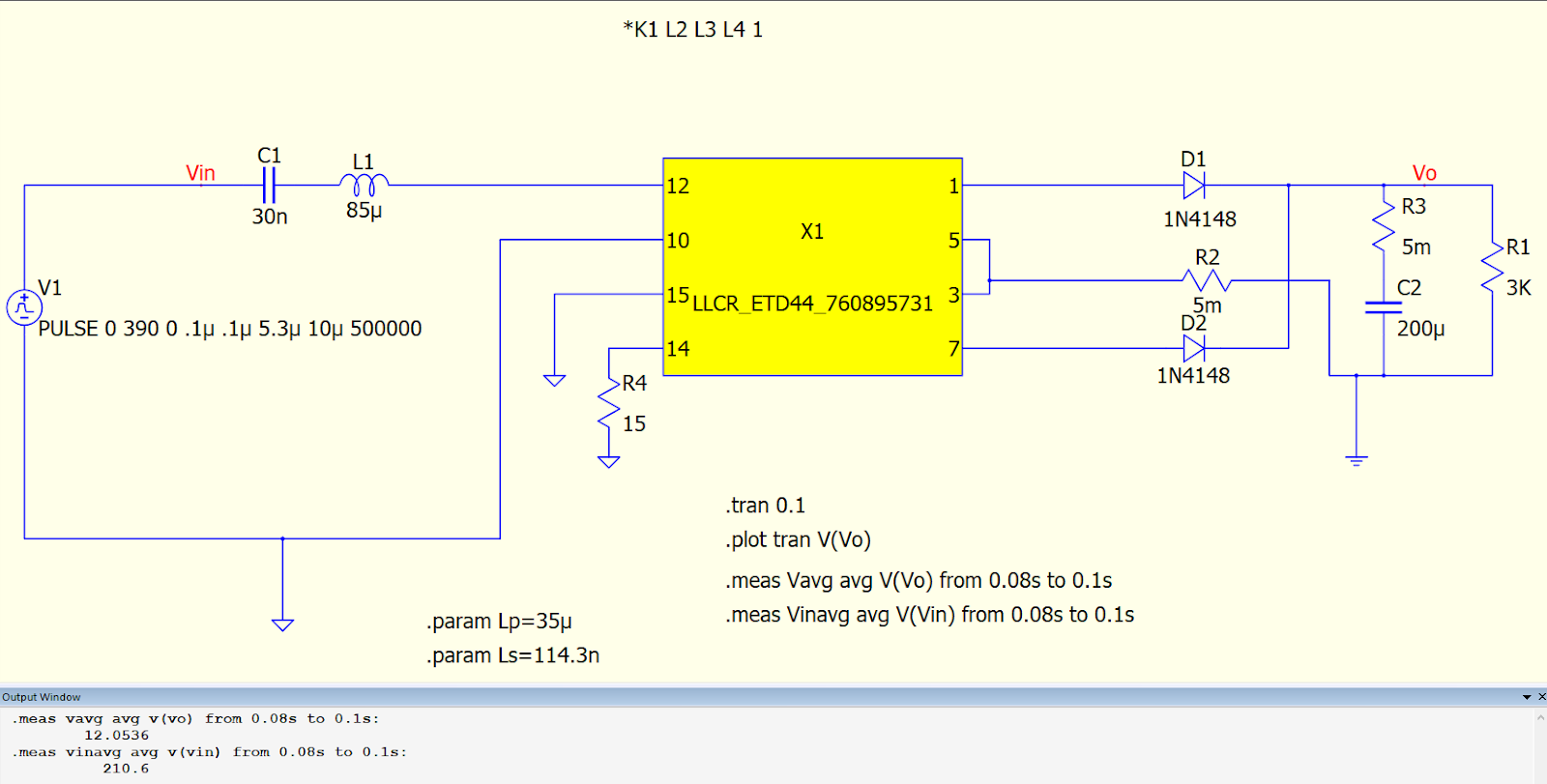
We have also been trying to find a custom resonant inductor but are having trouble finding one that meets our power requirements. Next steps are to get into contact with companies to discuss components that are not listed in their catalogs to general consumers or possibly custom magnetics.
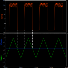
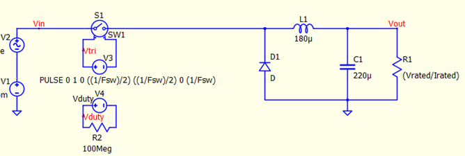
Buck Converters and Simulations
After the LLC converter steps-down the voltage from the PFC module to the isolated 12 volt rail, a solution for the 5 volt and 3.3 volt rails are next to be found. Utilizing the 12 volt rail, the 5 volt and 3.3 volt rails could be derived from it with the use of a step-down converter. To handle this process, Buck converters were chosen because of their high efficiency percentages and their relative simplicity. When determining the current rating that needs to be met for both the 3.3 and 5 volt rail, the Intel ATC Design Guide gives a recommended current rating of 30% of the rated output in amps. Because the 12 volt rail is rated at 50 amps out of the LLC, the recommended rated current for both the 3.3 and 5 volt rail is 15 amps. To ensure ourselves some overhead, we decided to spec the buck converter for 20 amps. Another important consideration is output ripple. The Intel ATC Design Guide states a maximum ripple of 50mV peak to peak for both the 3.3 and 5 volt rails. Our next steps are to finalize the selection of a buck converter IC that can meet our specifications.
Simulations
When looking at simulating the 3.3 and 5 volt rails, one immediate issue that arises is the difference in control structure that is possible in simulation vs what is typically seen in buck converter ICs. Most, if not all buck converter ICs utilize a form of a PID feedback controller to regulate the output voltage depending on load. Because of the complexity of introducing a proper PID controller into the simulation, the simulation focuses on how switching is handled and typical buck converter behavior, rather than authenticity to the behavior of a buck converter IC. However, it still aims to meet the current and ripple requirements which were specified above. The goal of this simulation is to serve as a resource to those less familiar with buck converters to better understand them and their role in the power supply.
- Simulation pictures are from the 12 volt to 5 volt buck converter.
Estimated BOM for the PCB
Because the case has not been fully finished, the costs for that are unsure at the moment and with us having issues finding magnetics for the LLC converter and thus not having final values for our passive components, some estimates had to be made. Average component value, package size, and rating requirements were used to find estimated prices for these unknown component values.
| Component Type | Total Qty. | Unit Cost | Total Cost |
| Resistor | 31 | 0.3 | 9.3 |
| Ceramic Capacitor | 12 | 0.25 | 3 |
| Electrolytic Capacitor | 12 | 0.6 | 7.2 |
| Inductor | 1 | 1.5 | 1.5 |
| Diode | 5 | 0.4 | 2 |
| Zener Diode | 3 | 0.5 | 1.5 |
| Rectifier | 1 | 0.7 | 0.7 |
| Common Mode Choke | 3 | 1.5 | 4.5 |
| N-Type MOSFET | 4 | 9 | 36 |
| PFC IC (UCC28056) | 1 | 2.95 | 2.95 |
| LLC Control IC (UCC256404) | 1 | 2.78 | 2.78 |
| LLC Resonant Converter | 1 | 22.74 | 22.74 |
| Opto-Coupler | 1 | 1.5 | 1.5 |
| Heat Sink | 2 | 6 | 12 |
| PCB Fabrication | 1 | N/A | 6.04 |
| C13 Receptacle | 1 | 3 | 3 |
| Power Switch | 1 | 4 | 4 |
| Total Cost: | 120.71 |
Functional Requirements
- The entire device will have design files originated partially from free and open source software.
- We used entirely free software to complete this project. For simulation we used QSpice due to it being very good at simulating switching power electronics, and for CAD we used Onshape which is a popular, easy-to-use web-based CAD tool. Unfortunately, neither of these are open source.
- The device SPICE simulation shall be able to meet the 600 W power rating.
- Our spice simulations along with the datasheets for our primary power-handling chips show that we will be able to meet the 600W power rating.
- The device SPICE simulation shall be able to operate with 115 Vac mains input.
- Our power supply is designed to work with a nominal input of 115 Vrms.
- The device SPICE simulation shall be able to output 3.3V, 5V, and 12V.
- Our main LLC converter has a 12 V output. We have Spice simulations for a buck converter that we’ll use to step 12 V down to 5 V and 3.3 V. To do so we’ll use two buck converters both off of the 12 V rail.
- The device case design shall have a footprint that meets the ATX specifications (150 x 86 x 140 mm).
- Our case design meets this requirement.
- The case of the device shall be partially 3d-printable with sheet metal inserts for grounding.
- Our case design meets this requirement.
- The device’s BOM should cost 20% less than an equivalent commercially available unit.
- Currently our estimated BOM is over the price of a comparable power supply on Amazon.
- The device design shall have a CPU power connector and 24 pin Motherboard connector.
- Our design is capable of supplying power for a 24 pin motherboard connector.
- The device case design shall have OSHE branding.
- Our case design has OSHE branding.
Value Added Goals
- The device design has overcurrent protection.
- Our design uses fuses for overcurrent protection.
- The device design has connectors for SATA and PCIe.
- Our design is capable of supplying power to SATA and PCIe connectors.
- The device is designed to be able to switch between 115 Vac and 230 Vac mains input.
- Our device is able to operate off of either 115 Vac or 230 Vac
- The device case design has screw holes that fit with ATX cases.
- Our case design has screw holes that fit with ATX cases.
- The device design has an ECO mode.
- Our device does not currently have an eco mode.
Health and Safety Concerns
Throughout the design process, concerns of health and safety were taken into consideration to ensure that the power supply is safe to build and utilize by an end user. Many of these safety guidelines, such as case design and wiring requirements were derived from the Intel ATX Version 3.0 Multi Rail Desktop Platform Power Supply Design Guide, Rev. 2.01 (February 2023).
Use of Free and Open Source Software
- Free resources that were used to design the power supply include LTSpice, QSpice, and Onshape.
- LTSpice and QSpice used for SPICE simulation for circuit modeling
- Onshape used for CAD design for ATX Case
- Open Source resources that were used include KiCad and Cura
- KiCad used for PCB schematic
- Cura used for slicing 3-D objects to be 3-D printed