
SPRING 2025
WEEK 14 UPDATE – Project Update 12
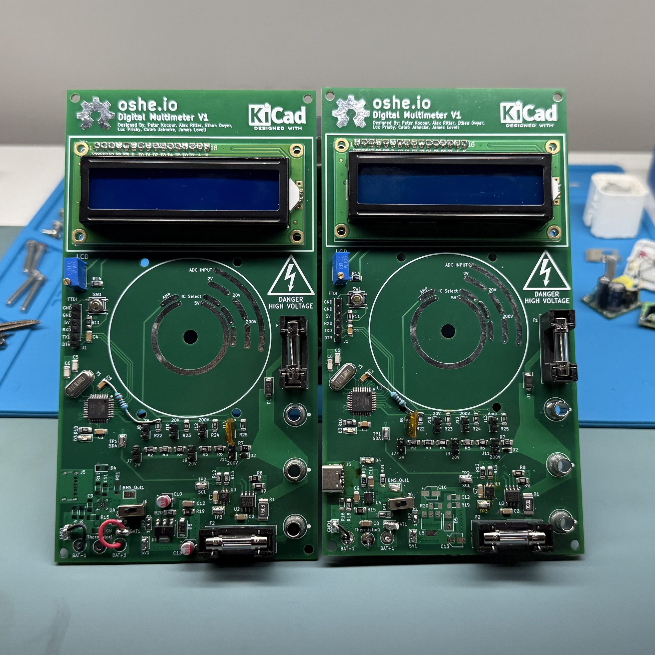
Final Project Photo
Week 14 Reflection:
This week our team met to review what we have written in the report and what’s remaining. So far, we have made some really good progress and there are just a few final touches to add next week!
To-Do List for Finals Week
- Finish our final report!!!
- Review what has been written
- Finish any remaining parts
Concerns for Finals Week:
None!
Posted Date: 04/20/2025
WEEK 13 UPDATE – Project Update 11
Week 13 Reflection:
This week’s progress isn’t all that exciting but as we are wrapping up the semester, we have been working on getting our final report drafted up and completed. So far we have a pretty good draft going with quite a bit of detail on how we went about creating the device and how it works. Next weeks goals will center around finishing up our final report prior to finals week.
To-Do List for Week 14
- Write documentation
- Finish our final report!
Concerns for Week 14:
Much like last week, I don’t really have any concerns for this week. Ideally, we will be able to knock out the remaining pieces of our final report prior to finals week as we already have a good chunk of the report done!
Posted Date: 04/12/2025
WEEK 12 UPDATE – Project Update 10
Week 12 Reflection:
This week was all hands on deck to make sure everything was ready to go for our project check-off. Our team met a few times to make sure we got all the minor issues in the code flushed out and made sure we had a plan for presenting our project. Wednesday was our project check off and everything went quite smoothly! Next up on the list will be wrapping up our project report and planning out next semester.
To-Do List for Week 13:
- Write documentation
- Do we want to document the research process or just the final components needed in the design?
- Maybe start writing up how a multimeter actually functions?
- Start writing our final report!
Concerns for Week 13:
I don’t really have any concerns for this week. Ideally, we will be able to knock out our final report so we don’t have to worry about it during week 14 and finals week but we will see how things go!
Posted Date: 04/06/2025
WEEK 11 UPDATE – Project Update 9
Week 11 Reflection:
We have assembled PCBs!!! This week was quite a productive one. Our team met several times in the Plexus Lab to get our final boards, shown above, assembled and functioning! Several of us were also working on getting the code working throughout the week and with a few small modifications to the PCBs, everything is working as it should. Speaking of modifications, we did discover a few issues with our design. The first problematic issue was the missing bootloader pins which are required to initially load the Arduino Bootloader onto the microcontroller, where then we can program them through the 6 pin header on the left side of the board. Thankfully, all of the bootloader pins are also being used for different peripherals so we were able to just solder on a few temporary wires, get the bootloader programmed onto the ATMEGA processor, and then remove those wires. The next issue we ran into was with the mode selection resistor divider. Somehow, all of us managed to completely forget to add a fifth resistor to create the actual resistor divider. Instead, we just had 5 different resistors all connected to the same pin, meaning none of them ever had a path to ground through another resistor, meaning none of them ever showed a voltage drop like they were supposed to. However, with the quick addition of a 1k ohm resistor, even that is now working as intended. To wrap up the week, I quickly reviewed our project spec and checked off the final task, creating a test circuit for our device. I made a quick schematic in KiCAD with a resistor divider to measure current through, and another resistor divider with an LED to measure the voltage drop across. We have officially checked everything off on our project specification!
To-Do List for Week 12:
- Breadboard our test circuit for our checkoff on Wednesday!
- Put a procedure together for our Wednesday Checkoff.
- Write documentation
- Do we want to document the research process or just the final components needed in the design?
- Maybe start writing up how a multimeter actually functions?
- Start writing our final report!
Concerns for Week 12:
My only concerns for this week is whether or not we will be able to fix the slight error in our voltage measurements at the 20 volt and 200 volt ranges, how that could affect our project checkoff, and generally how our project checkoff will actually go. Fixing the issues in the 20 volt and 200 volt ranges shouldn’t be too hard, we just have to play around with the conversion factors in the code, but I haven’t quite been able to figure out how the conversion factor I have from our resistor divider is not correcting the voltage correctly.
Posted Date: 03/30/2025
WEEK 10 UPDATE – Project Update 8
Week 10 Reflection:
Progress was limited this week as we are waiting for the boards to arrive. We did, however, receive our parts from Digikey so we are ready to go for assembly once our boards arrive. Alex and I met to work on some of the code with the LCD and current measurement ADC. Alex had a good chuck of the code functioning already so most of our work was with integrating the current measurement ADC into the code so the measurements would be displayed on the LCD. We did get this functioning which was great news and now all that’s left is to incorporate the rest of the voltage measurement code into what we already have.
To-Do List for Week 11:
- Work the rest of the team to develop our code and get it functioning on a breadboard prototype.
- Complete a full breadboard replica of our PCB design
- Double check that we didn’t miss anything on the PCB
- Write documentation
- Do we want to document the research process or just the final components needed in the design?
- Maybe start writing up how a multimeter actually functions?
Concerns for Week 11:
Originally my big concern for Week 11 was getting the voltage measurement board and code working as James and Caleb were running into some issues getting that board to read any measurements. However, just earlier today they have managed to get the ADC working and reading the correct data. Thus, my big concern for this week is getting our PCB assembled and hoping that everything works when we go to upload the code and test things out.
Posted Date: 03/22/2025
WEEK 9 UPDATE – Project Update 7
Week 9 Reflection:
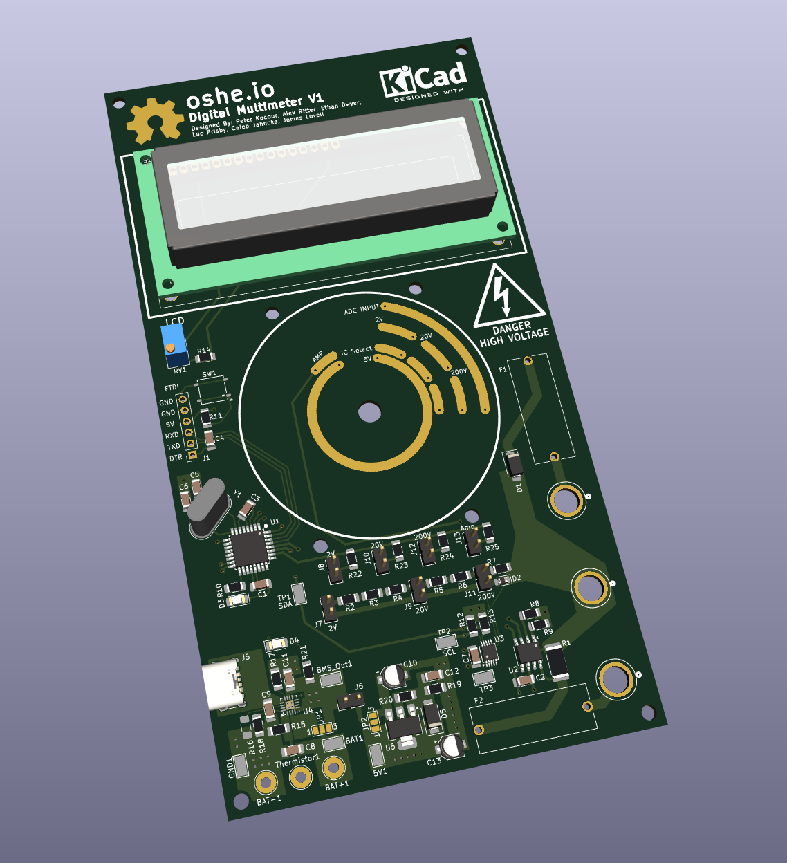
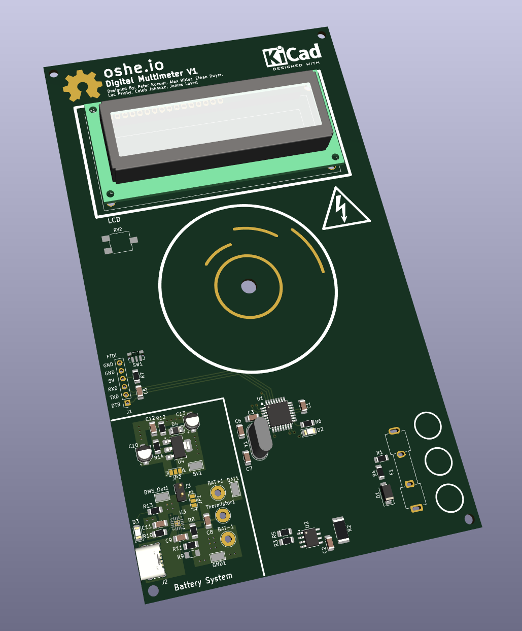
We finally completed the PCB!!! Above is a photo of our completed Version 1 design. As a team, we met several times throughout the week to finalize everything needed to wrap up the board. We sent the board off to Carson Belyk for review and he sent back a 20 slide presentation of things we should take a look at fixing prior to ordering the boards. Many of the highlighted issues were unproperly routed traces, including many 90 degree bends which is largely frowned upon. We also had some issues with clearances, trace widths, and via placements that were fixed as well. Parts wise, I met with Eric Riebe who found several of our parts already in stock in the OSHE Lab, which dramatically cut down on the cost of parts for our boards. That led us to Friday, were we placed the order for our boards through JLCPCB and the order for our parts through Digikey.
To-Do List for Week 10:
- Work the rest of the team to develop our code and get it functioning on a breadboard prototype.
- Create breadboard prototype
- Double check that we didn’t miss anything on the PCB
- Write documentation
- Do we want to document the research process or just the final components needed in the design?
- Maybe start writing up how a multimeter actually functions?
Concerns for Week 10:
My big concern for the next two weeks are how long it’ll take for our PCBs to show up from JLCPCB and whether or not we will be able to finish the code in time for our boards arriving. Unfortunately, we don’t have much control over the former, but we can work diligently to get the code working on a breadboard prototype prior to board arrival to hopefully save us some time troubleshooting any issues.
Posted Date: 03/16/2025
WEEK 8 UPDATE – Project Update 6
Week 8 Reflection:
Week 8 was probably one of the most productive weeks of the project. We met several times throughout the week to plan out the last steps of the PCB design and get our presentation put together for the OSHE meetings. On Friday, we all met as a group for several hours to sit down and work out the last few remaining issues in our design and hopefully wrap it up. Unfortunately we didn’t get the PCB design 100% complete during this meeting, however, we did flush out a lot of the remaining questions, got the majority of the schematic finished, and Luc put a ton of effort into finishing up the PCB dial design. We also started to add several of the custom footprints into the design which helped us get an idea of how many components we had to start finishing up component placement and board layout
To-Do List for Week 8:
- Finalize the entire schematic
- Are component values correct?
- Do all components have a PCB footprint assigned?
- Is every component (voltage measurement, current measurement, etc) present on the schematic?
- Finalize Bill of Materials
- Complete PCB design
- Finish component placement/board layout
- Have Carson Belyk review our design before sending it off for production.
- Start writing documentation
- Do we want to document the research process or just the final components needed in the design?
- Maybe start writing up how a multimeter actually functions?
Concerns for Week 8:
My original concerns for this project have started to subside. Instead, my primary concern is making sure both the voltage measurement IC and the current measurement IC have the current resistor values for their I2C communication lines as to not interfere with each other. That being said, a potential solution to this problem could be adding resistors to both lines on both ICs that go to both 5 volts and ground, allowing us to populate or not populate certain resistors based on what SDA or SCL line needs to go to. This could allow us to easily correct a mistake, if one is made, without the problem of having a board already manufactured for a certain configuration .
Posted Date: 03/09/2025
WEEK 7 UPDATE – Project Update 5
Week 7 Reflection:
Week 6 and Week 7 were pretty productive. I got the battery management schematic, the microcontroller schematic, and a majority of the PCB complete. I started a Bill of Materials for the project and started to pick out the required components from Digikey. We were also approached by the enterprise program to submit an application for Milwaukee Tool, of which, we completed and set off, hoping to hear some good news in the future!
Unfortunately the PCB design is still not complete so we didn’t get the chance to review it with Carson Belyk review it over spring break, however, he is still on board and available to review it when it is completed!
To-Do List for Week 8:
- Finalize the entire schematic
- Are component values correct?
- Do all components have a PCB footprint assigned?
- Is every component (voltage measurement, current measurement, etc) present on the schematic?
- Finalize Bill of Materials
- Are there any parts unaccounted for?
- Display?
- Banana Plugs for leads?
- Power switch?
- Are there any parts unaccounted for?
- Complete PCB design
- Have Carson Belyk review our design before sending it off for production.
- Start writing documentation
- Do we want to document the research process or just the final components needed in the design?
- Maybe start writing up how a multimeter actually functions?
Concerns for Week 8:
My overwhelming concern is still whether or not we will be able to stay on track to have a functioning PCB by the end of the semester. While we are behind where I hoped we’d be, we are still on track to have a PCB design ordered well before the end of the semester, but the longer we wait the less time we will have to troubleshoot and/or reorder a revised PCB if needed. That being said, we have several meetings set up for this week to finalize the PCB and BoM to be reviewed this weekend with Carson and hopefully get sent off for production next Monday!
Posted Date: 03/03/2025
WEEK 5 UPDATE – Project Update 4
Week 5 Reflection:
Last week I had originally selected the BQ24072TRGTR IC for our battery management system. After a closer look at the data sheet, I found the BQ24075RGTR IC would be a better fit for our system. The 24075 has a regulated 5.5 volt output, meanwhile the 24072 only has a 3.72 volt output. With the increase to 5 volts, it became easier for us to provide two power options to users. One option would be to use a rechargeable battery and this IC and the other would be to use a 9 volt battery and a TI LM317 voltage regulator. This selection would be accomplished two ways. One would be through the use of solder jumpers during assembly, and the other would involve simply not populating the components for the option you chose NOT to go with. For example, if you chose the 9 volt and LM317 route, you wouldn’t need to populate the BQ24075RGTR or any of its corresponding components.
Unfortunately didn’t get a PCB design done by CDR. However, we now have a GitHub repository for our KiCAD files, allowing each of us to update separate pages of a schematic and have it auto-update the primary schematic. This should hopefully allow us to pretty quickly develop a PCB design by the end of the week and have it sent off for production during spring break!
To-Do List for Week 6:
- Finalize schematic
- Are component values correct?
- Do all components have a PCB footprint assigned?
- Finalize Bill of Materials
- Are there any parts unaccounted for?
- Display?
- Banana Plugs for leads?
- Power switch?
- Are there any parts unaccounted for?
- Complete PCB design
- Have Carson Belyk review our design before sending it off for production.
- Start writing documentation
- Do we want to document the research process or just the final components needed in the design?
- Maybe start writing up how a multimeter actually functions?
Concerns for Week 6:
My overwhelming concern at the moment is being able to complete a PCB design by the end of week 7 in time for spring break. We are already half way through this semester and the deadline for this project is not far away. That being said, if we can complete a design by the end of this week, I can work with Carson to review it in the beginning of spring break with the hope of sending them off for production by the end of spring break.
Posted Date: 02/16/2025
WEEK 4 UPDATE – Project Update 3
Week 4 Reflection:
I made some pretty good progress this week on the battery management side of things. After selecting the Texas Instruments BQ24072TRGTR IC, I started working on creating a schematic and hoping to move onto creating a PCB in the coming week. I also want to work on integrating a way to switch off the battery management system and instead use just a 9 volt battery or two AA batteries instead. The team has also set up some times for the coming week to put a Critical Design Review presentation together. My original hope was to have a PCB design made for CDR, which is still possible, but I’m not completely sure that will happen in time. Instead, I see schematics being complete in time and saving the PCB design for after CDR.
To-Do List for Week 5:
- Look into BMS ICs
- What if we also wanted the ability to use a 9 volt battery, can it bypass the BMS?
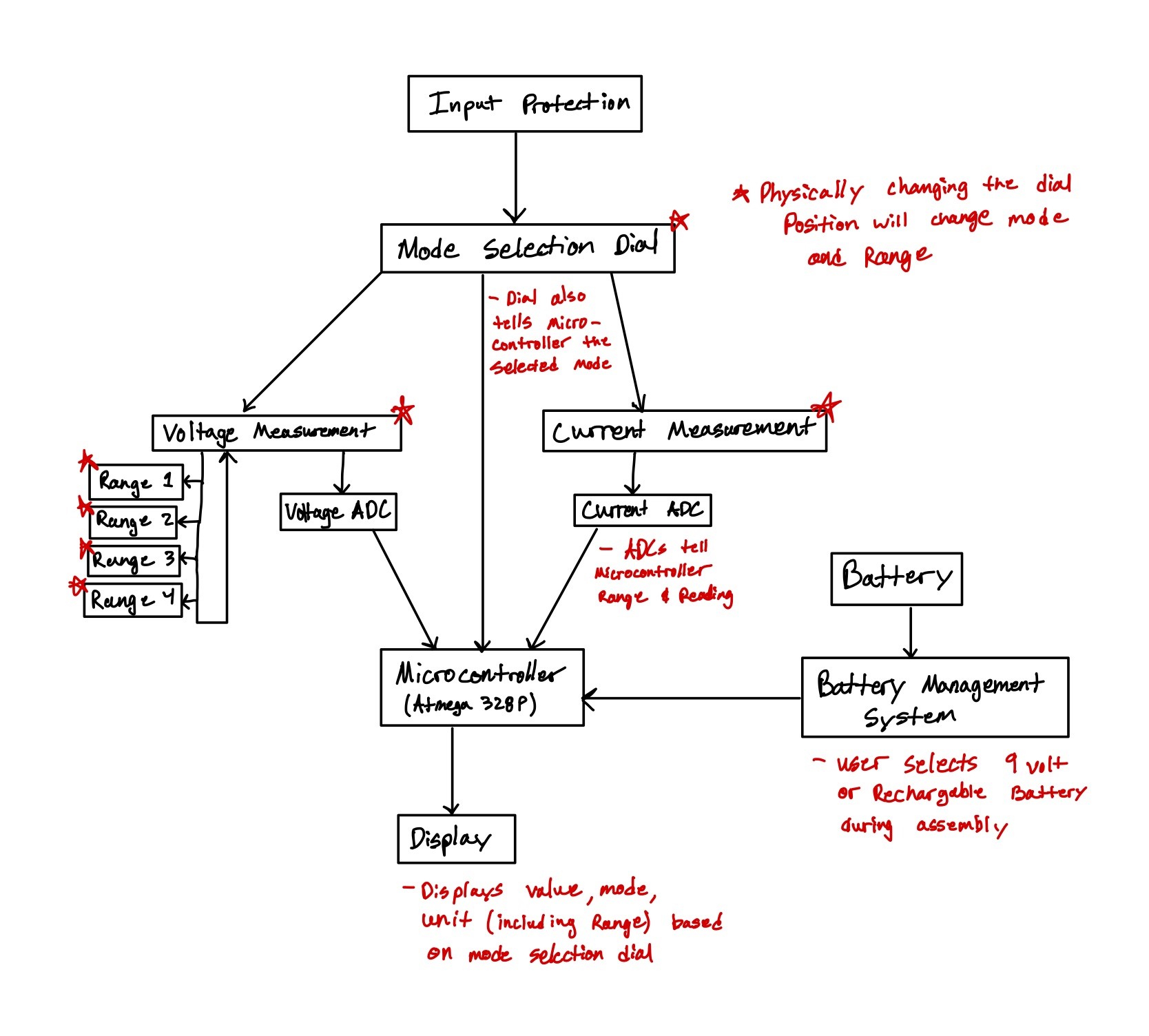
- Make a block diagram for our project
- What systems need to be on the block diagram?
- How do I want to organize the diagram? Is there a flow to the system?
- Start writing documentation
- Do we want to document the research process or just the final components needed in the design?
- Maybe start writing up how a multimeter actually functions?
Concerns for Week 5:
My biggest concern is still ensuring that we stay on schedule and don’t fall behind. I don’t think we’d be able to reach my initial goal of having a PCB design created in time for CDR, but hopefully we can at least have a schematic ready to go. My other concern on cost of our meter is slowly becoming less of a concern. While there are still some ICs and other components that could be a little pricy, I think we will still be under the $30-50 range that I am aiming for if someone were to recreate just one of these. The goal is still to keep the cost even lower, preferably under $20 if several were being made at once.
Posted Date: 02/03/2025
WEEK 3 UPDATE – Project Update 2
Week 3 Reflection:
We made some great progress this week! After some discussion, we decided to switch from the ICL7107 IC to the ATMEGA328P IC for the primary brains behind our DMM. The ICL7107 lacked much of the customizability that the 328P supports, was $18-20 more expensive, and there wasn’t a lot of documentation on it. Meanwhile, the ATMEGA328P was super easy to find, being the brains of many Arduinos currently on the market, was much cheaper at just $1.50-2.50 each, has tons of customizability as well as documentation, making this choice a no-brainer. We also have a rough plan for how we plan to split up the project. Dividing up the project into sections like creating the case and mode selection switch, creating the battery management system, and creating the primary circuitry responsible for measuring and displaying voltage, current, and resistance. To wrap up the week, we also settled on what times we were available for CDR in a few weeks.
To-Do List for Week 4:
- Look into BMS ICs
- Do we want to use an 18650 cell?
- How about a smaller one cell LiPo?
- What if we also wanted the ability to use a 9 volt battery, can it bypass the BMS?
- Make a block diagram for our project
- What systems need to be on the block diagram?
- How do I want to organize the diagram? Is there a flow to the system?
- Start writing documentation
- Do we want to document the research process or just the final components needed in the design?
- Maybe start writing up how a multimeter actually functions?
Concerns for Week 4:
My biggest concern is ensuring that we stay on schedule and don’t fall behind. My goal is for us to have a PCB design created in time for CDR, allowing us to receive some feedback on our design and make the necessary changes, prior to ordering boards and components. My second big concern is the overall cost of our meter. Some of the ICs and other components that we are finding can get a little pricy, potentially pushing the cost of recreating this project somewhat higher than we are hoping for.
Posted Date: 01/25/2025
WEEK 2 UPDATE – Project Update 1
To-Do List for Week 3:
- Decide on IC for DMM
- Do we want to stick with the ICL7107?
- What about using the ATMEGA328P from an Arduino, similar to existing Open Source Designs
- Divide up the project into individual or groups assignments
- Maybe have one or two people working on the case?
- Two to three people on integrating the IC with the ADC and other necessary components?
- Two to three people working on the battery system?
- Do we just want to stick with a 9 volt or two AAA batteries?
- Do we want to create a Battery Management System for a rechargeable battery?
- Sign up for CDR
- When is everyone available based on the available time slots?
Concerns for Week 3:
I have two primary concerns for the upcoming week. The first big concern is how we can divvy up the project into individual or small group sections. I have a few ideas based on how we wrote the project spec but it’ll mostly be up to the team. My other big concern for this upcoming week is being able to find a time that we are all free for CDR based on the available CDR times. There are a few possibilities but again this will be up to the team and their availability.
Posted Date: 01/21/2025
WEEK 1 UPDATE
- Begin the Digital Multimeter Project
- Met with the DMM Team
- Completed the DMM project specification
- Began research into ICs and started planning out the DMM project
Posted Date: 01/13/2025
FALL 2024
WEEK 5 UPDATE – Project Update 3
Week 5 Reflection
This past week consisted primarily of house keeping items. I spent time with cleaning up my schematics so they follow proper technique. I made some modifications to the schematics based on some feedback from the team, such as condensing certain sections and combining things that were used by both the 5 volt and 3.3 volt schematics. In addition to that, I also made some updates to my bill of materials and further updates to the schematic. I have put together a pretty solid initial BOM based largely on the Texas Instruments evaluation board as well as updating all of the footprints on each of my components in my schematics, which was great preparation for board layout design this upcoming week.
To-Do List for Week 6
- OVERALL GOAL: Board layout design, and preparation for board manufacturing.
- Board Layout Design Sub Goal – Create a board layout in KiCAD that meets all necessary requirements per the manufacturers datasheet and fits within sizing constraints (once those are determined), to do so I must:
- Create and/or reference some type of list of requirements based off the manufacturers datasheet.
- Reference the provided recommended typical application board layout for an initial design.
- Alter BOM and part selection if any components were switched to a different footprint size, such as switching from 0805 to 0603.
- Prepare For Board Manufacturing Sub Goal – Ensure everything is prepared for boards to be ordered and manufactured, to do so I must:
- Double check all my work with my team members to ensure that all potential issues or mistakes are caught and addressed before board manufacturing.
- Make any necessary or recommended design changes.
- Return to my team members to double check my board again.
- Repeat process until every team member is satisfied with the state of the board and ready for it to be put into production.
Week 6 Concerns:
My week 6 concerns assign similarly to last weeks. I am concerned about how to properly create multi-layered boards with large planes for things like the main grounding plane. As well as, the second being the ability to fit both buck converter designs into the rough dimensions of a note card, allowing the back of the board to contain our modular cable connectors.
Posted Date: 09/29/2024
WEEK 4 UPDATE – Project Update 2
Week 4 Reflection
Last week’s to-do list was ambitious. I set out to do a lot in a week that I quickly discovered became quite busy. Despite this, I still managed to complete half of my very lengthy to-do list.
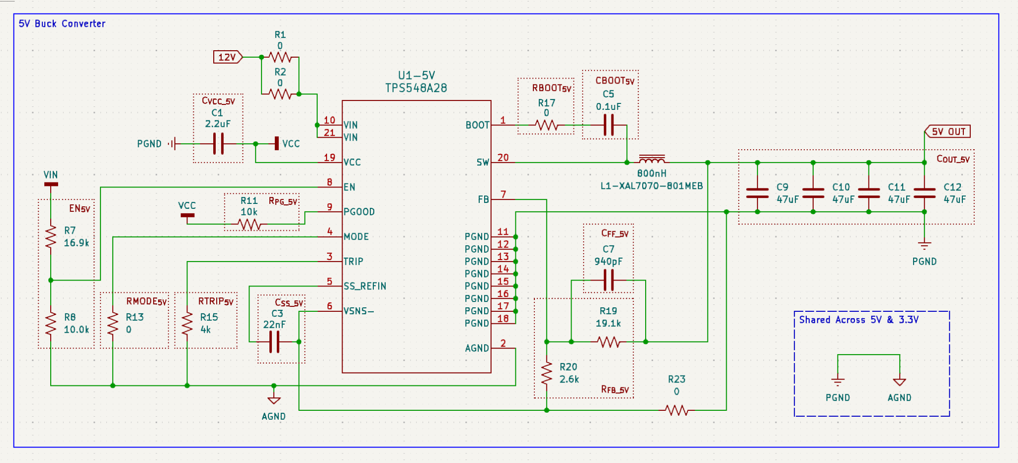
I started with altering the original 2.5 volt schematic to step 12 volts down to 5 volts and 3.3 volts via the recommendations set my the Texas Instruments Excel calculator. Utilizing this calculator not only gave me the necessary values for resistor 1 and 2, but also provided me with the values for every component in each schematic. Meanwhile, the calculator also checked that the selected and calculated component values would perform correctly to step down 12 volts to 5 volts and 3.3 volts while also maintaining a 15 amp current output. This proved to be harder than initially expected as I ran into several issues with the selected inductor limiting our potential current output. Through discussions with my team, we discovered that it was calculating this expected outcome with a huge input voltage range, instead of using the already refined input voltage range from our other boards. After altering this voltage input range, our selected inductors would adequately perform under our set parameters. With this change in mind, I quickly incorporated the few component value changes and finished the 5 volt and 3.3 volt schematics.
After completion of the schematics, I moved onto component selection. Through the use of the Texas Instruments calculator, most of the components and their values were already selected for me, but there were still a few components that I had to settle on. The values of the inductors were already selected, but I had to find physical components that could actually provide the theoretical numbers. I chose to selected not only the recommended 800nH inductor from Coilcraft for the 5 volt circuit, which also happened to be used in the evaluation board from Texas Instruments, but I also chose a 600nH inductor from Coilcraft for the 3.3 volt circuit as well. As for the rest of the components, I chose a standard 0805 footprint for board layout design and will alter the components footprint and bill of materials once the board layout has been complete, just in case a few components are switched to a 0603 sizing to save space.
To-Do List for Week 5
- OVERALL GOAL: Finish both 5 volt and 3.3 volt schematics, part selection, board layout design, and preparation for board manufacturing.
- Board Layout Design Sub Goal – Create a board layout in KiCAD that meets all necessary requirements per the manufacturers datasheet and fits within sizing constraints (once those are determined), to do so I must:
- Create and/or reference some type of list of requirements based off the manufacturers datasheet.
- Reference the provided recommended typical application board layout for an initial design.
- Alter BOM and part selection if any components were switched to a different footprint size, such as switching from 0805 to 0603.
- Prepare For Board Manufacturing Sub Goal – Ensure everything is prepared for boards to be ordered and manufactured, to do so I must:
- Double check all my work with my team members to ensure that all potential issues or mistakes are caught and addressed before board manufacturing.
- Make any necessary or recommended design changes.
- Return to my team members to double check my board again.
- Repeat process until every team member is satisfied with the state of the board and ready for it to be put into production.
Week 5 Concerns:
I only have two big concerns for week 5. The first is learning how to properly create multi-layered boards with large planes for things like the main grounding plane. Then the second is being able to fit both buck converter designs into a small area on the back of the board with our modular cable connectors.
Posted Date: 09/22/2024
WEEK 3 UPDATE – Project Update 1
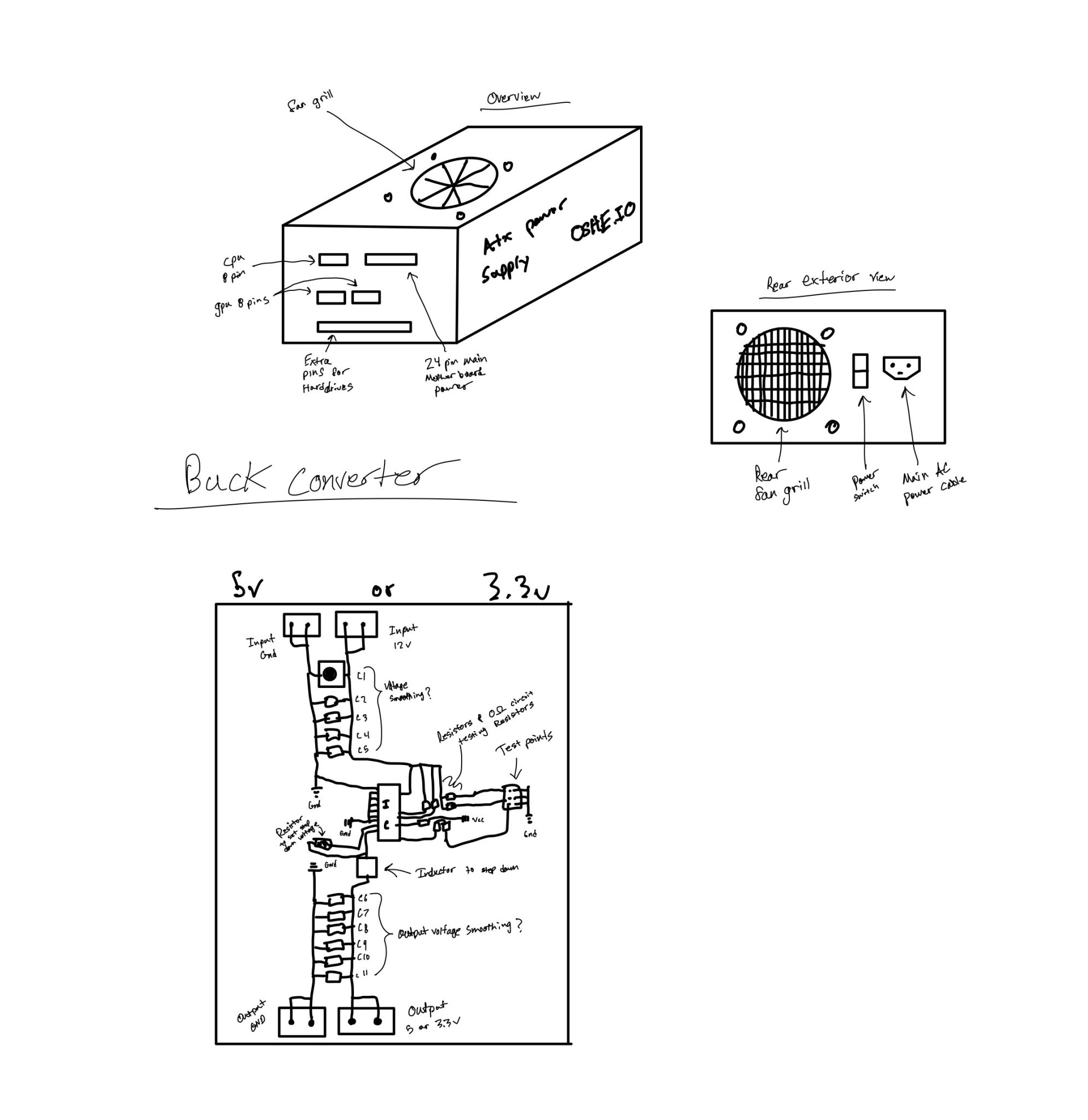
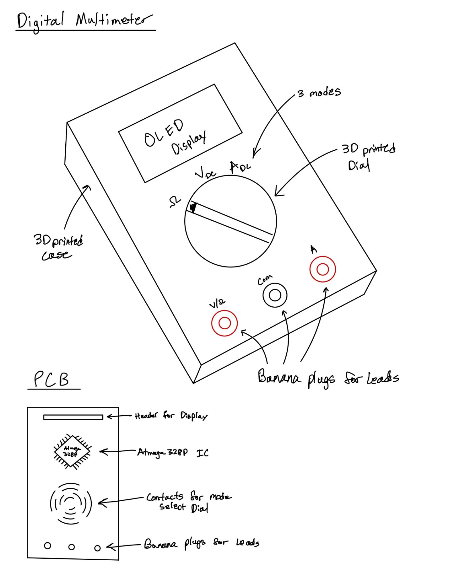
Image Above: Rough sketch of expected final project design as well as general schematic/layout for buck converter.
To-Do List for Week 4
- OVERALL GOAL: Finish both 5 volt and 3.3 volt schematics, part selection, board layout design, and preparation for board manufacturing.
- Schematic Sub Goal – Alter my current schematic to step down from 12 volts to 5 volts instead of the step down to 2.5 volts, to do so I must:
- Alter resistor 1 to set the buck converter IC to convert 12 volts down to 5 volts instead of the initial design that follows the datasheets typical application of 2.5 volts.
- Utilize Texas Instruments provided Excel calculator to assign the typical input voltage of 12 volts and the wanted output of 5 volts and 15 amps.
- Incorporate the calculators recommendations into my initial schematic.
- Part Selection Sub Goal – Select parts that align with my newly updated schematic, to do so I must:
- Start with the typical application parts list and alter parts based on my updated schematics.
- Ensure my part selections are no smaller than the 0603 footprint to allow for hand soldering to be possible without major difficulty.
- Board Layout Design Sub Goal – Create a board layout in KiCAD that meets all necessary requirements per the manufacturers datasheet, to do so I must:
- Create and/or reference some type of list of requirements based off the manufacturers datasheet.
- Reference the provided recommended typical application board layout for an initial design.
- Alter the initial typical application board layout to fit the 0603 or larger footprints and ensure that there is adequate room to hand solder.
- Prepare For Board Manufacturing Sub Goal – Ensure everything is prepared for boards to be ordered and manufactured, to do so I must:
- Double check all my work with my team members to ensure that all potential issues or mistakes are caught and addressed before board manufacturing.
- Make any necessary or recommended design changes.
- Return to my team members to double check my board again.
- Repeat process until every team member is satisfied with the state of the board and ready for it to be put into production.
Posted Date: 09/12/2024
WEEK 2 UPDATE
- Selected the TPS548A28 as the buck converter IC of choice for our application.
- Created the initial buck converter schematic in KiCAD based on Texas Instrument’s datasheet for the TPS548A28.
Posted Date: 09/12/2024
WEEK 1 UPDATE
- Started my first week in OSHE!
- Started reviewing the plans for the buck converter selection
Posted Date: 08/30/2024