
Week of April 13
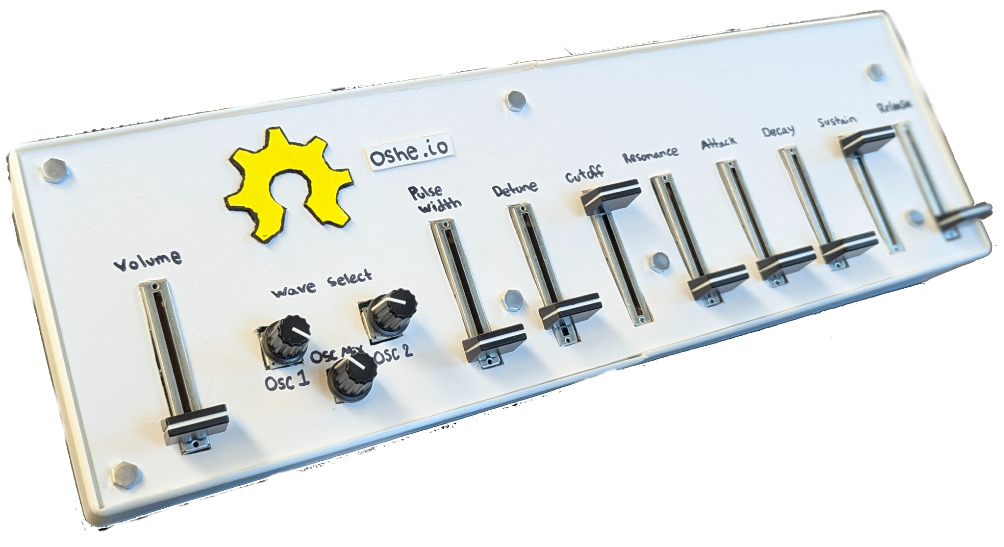
This week I worked on cleaning up the code for the synth and testing and uploading the final version of the firmware to the OSHE github. I also worked on helping clean out our project drawer a bit. The rest of my time I spent revising and adding to our final report. An image of what the final assembled prototype looks like:
Next week, my tasks will be:
- Work on finishing the final report
- Make sure all project files are uploaded to the github/open source repository
Week of April 6
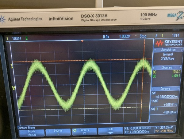
This week I worked on gathering characterization data for the headphone level sound output to ensure it complies with industry standards. We were able to confirm that the peak-to-peak voltage at max volume is well within the 1 V standard, and it is centered around 0 V according to the standard. I also wrote my sections of the final report for the first draft and worked with the rest of the team recording our section of the Design Expo video and making our section of the poster.
Next week, my tasks will be:
- Make needed revisions and additions to the final report
- Prepare for Design Expo on Tuesday
Week of March 30
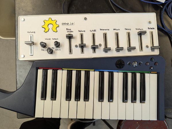
This week I worked with Ian and Tom on getting the enclosure finished and ready for Lily to make a lid for it. We welded the two halves of the printed enclosure together with glue and measured out where we would need holes for I/O. I also spent some time testing the external power input and confirmed its functionality, as well as the data breakout port so the Teensy can still be programmed from the external USB port on the case. I also made some final updates to the firmware so that all the physcial controls modified their assigned parameters correctly. We were able to complete everything on our project spec in time for checkoff. After checkoff, I perfromed an extended 2-hour testing session with the synth to confirm reliability, and I observed no major issues while testing as many edge cases I could think of during this time.
Next week, my tasks will be:
- Gather quantitative data for the headphone output levels for the final report
- Begin drafting final report
- Work with team on video and poster for Design Expo
Week of March 23
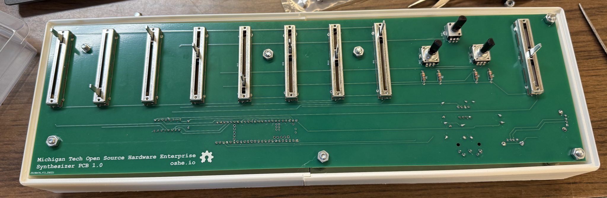
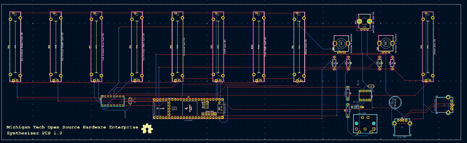
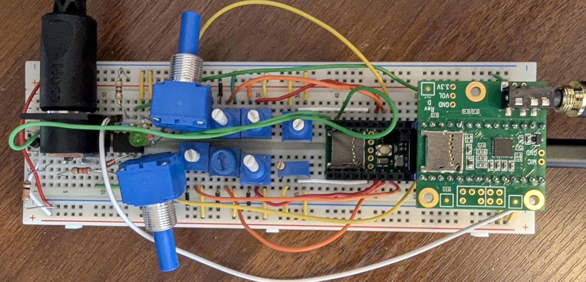
This week the PCB came in so I did an initial inspection of it and could not find any functional issues with it, so I spent a good chunk of my time this week soldering all the components onto the board and testing all the functionality of the synth. I was able to test all of the functionality of the instrument except for the external power input, since I did not have the correct cable but that will be a minor thing to test. All of the parameters of the synth itself seem to be working properly the best that I can tell. The only mistake made on the PCB was that our MIDI input port is facing backwards into the board rather than outwards from it, which will make plugging into it slightly cumbersome, but it does not affect functionality. It is looking like we will be able to finish all of our functional requirements in time for checkoff on Thursday. Here is an image of what the prototype currently looks like (technically upside-down) as well as an updated sketch of what our project will hopefully look like by checkoff time:
The only changes from our sketch at the start of the semester is the addition of oscillator 2, pulse width (for the pulse waveform), oscillator 2 detune and filter resonance parameters. The addition of these parameters was largely made possible by switching to a fully DSP implementation of the instrument instead of attempting to implement analog signal path elements into the design. The other change from the original sketch is that we will not be adding any sort of display, since every parameter has a dedicated control so it would be unnecessary and add complexity and cost.
Next week, my tasks will be:
- Work with the team to develop a solution for adding a lid to our enclosure
- Figure out a solution for testing the external power input
- Finish assembling the final prototype and complete all testing in time for project checkoff
Week of March 16
This week I made the orders for the PCB from JLCPCB and all the components we will need to populate the board. I also assisted the team with figuring out the direction we will be going for the enclosure. We will attempt to create a fully 3D-printed case, though it will have to be printed in two pieces due to the length of the PCB. Other than that, there has not been much to do this week besides wait for the PCBs and the parts to come in to solder and test the board.
Next week, my tasks will be:
- Solder components onto the PCB and test functionality
- Make any changes/fixes necessarry to the PCB
- Assist team with finishing the enclosure so we can build the final prototype
Week of March 9
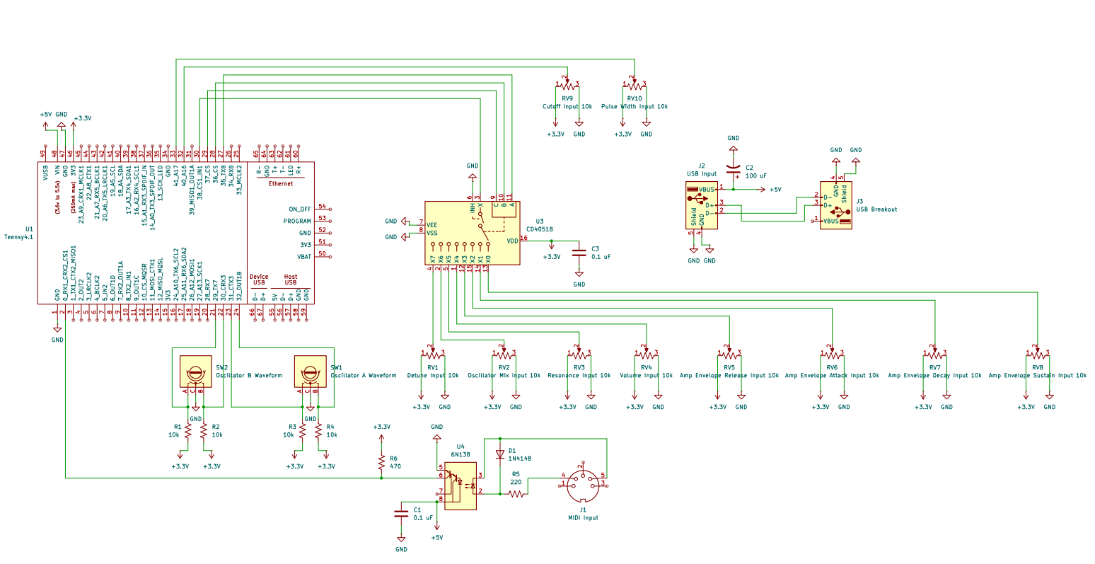
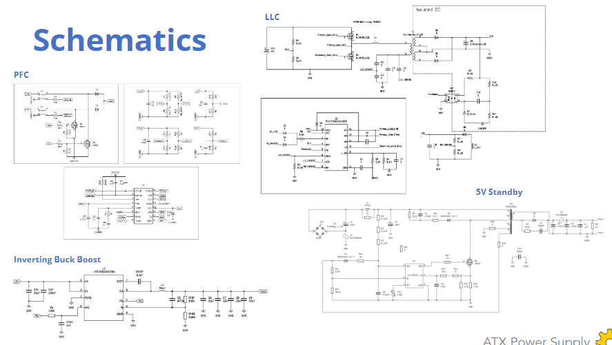
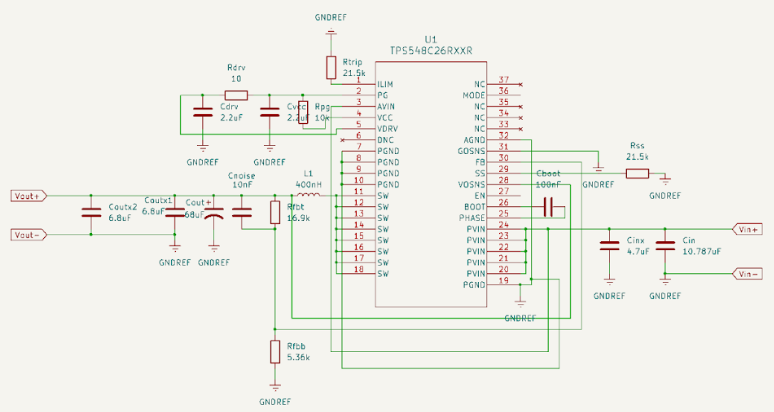
This week I worked on creating the electrical schematic for our final full-system design in KiCad, showing all the connections we would need between all the componenents that will be housed on our PCB. I also finalized the exact parts we would use for all of the components so I could find footprints for them and put them in the PCB design. After Lily finished with the PCB design, I reviewed it and made some minor edits, and hopefully we can get the board ordered this week. Here is a picture of the KiCad schematic and board design in their current state:
Next week, my tasks will be:
- Make any last changes needed to the PCB design and get it ordered from JLC PCB
- Finalize component part list and get all components we will need on the PCB ordered
- Figure our what we are going to do for the enclosure solution (fully 3D printed, metal, wood?)
Week of March 2
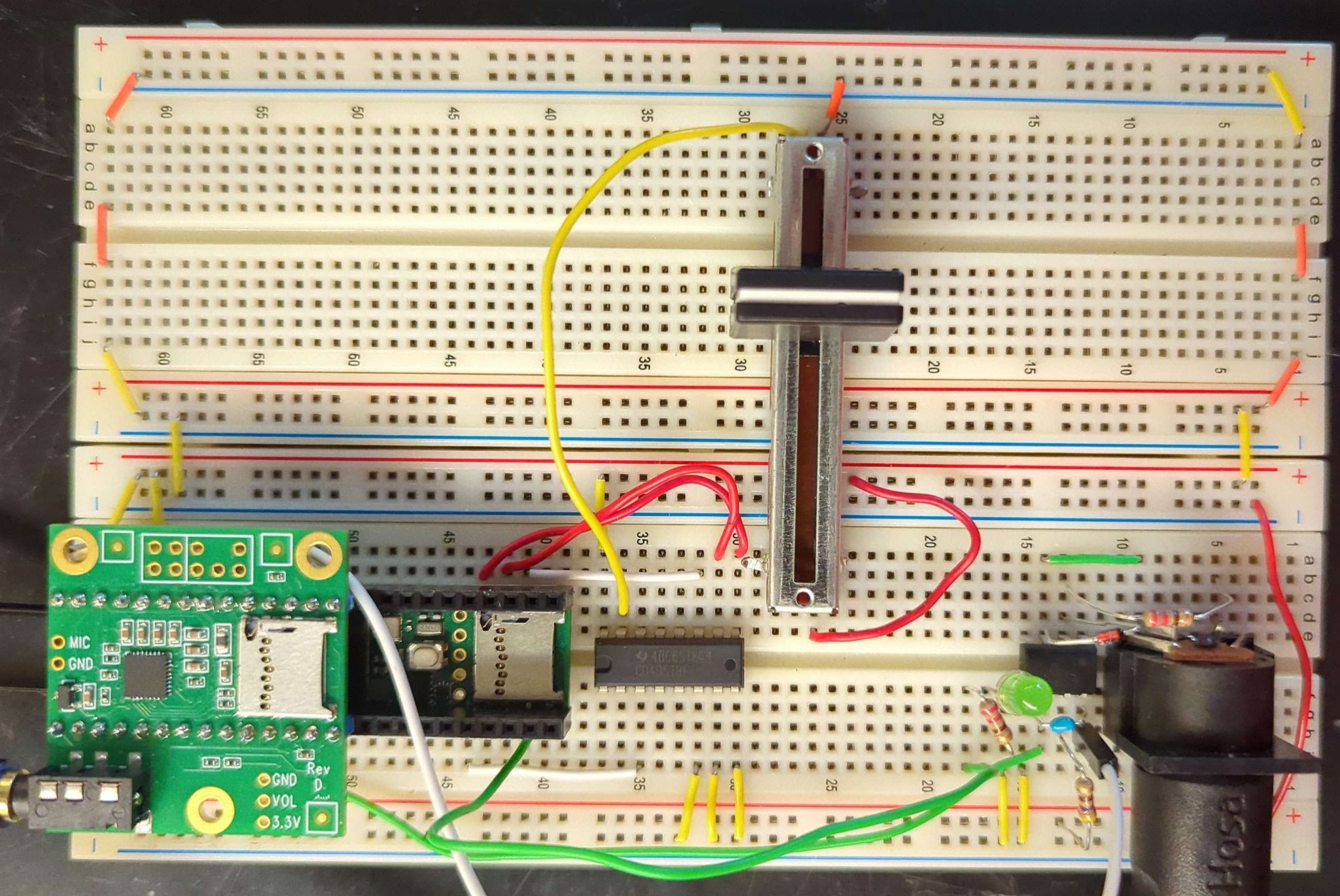
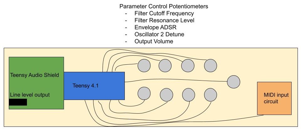
This week I worked on implementing the user control scheme using slider pots and a multiplexer for the analog inputs, as this is the solution we decided on. After wiring the prototype, I updated the firmware to scan through all the mux inputs to read each current pot value. The test was successful and we can move forward with this design for the analog inputs. I also implemented the rotary encoder as the physcial control for changing the base waveform, which is currently functional as a unidirectional control, meaning the waveforms are only iterated through one way (I plan to make it bidirectional in the future). Here is an image of the updated prototype testing the slider pot and mux:
Next week, my tasks will be:
- Assist Lily and Ian with PCB design. They made progress this weekend getting the component footprints in KiCad, and now a schematic will need to be made and traces laid out
- Finalize the power supply circuit so that can be added into the PCB design
Week of February 16
This week I mainly worked on designi ng the user control circuitry. As a team we decided to go with slider potentiometers as the main analog input, so I spent time researching the best solution for this and ordered some options to try. We will likely use logarithmic audio curve potentiometers, since the audio curve makes more sense for the parameters of a synthesizer. Here is an image of the actual functional prototype as it is currently implemented:
Next week, my tasks will be:
- Finalize the user control circuitry so that PCB design can begin for that portion of the synthesizer
- Work on the power supply design so PCB design can begin for that portion of the synthesizer
Week of February 9
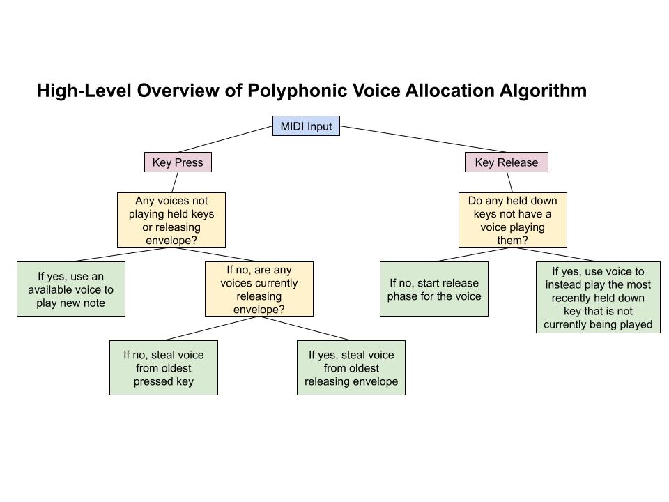
This week I worked on the polyphonic voice allocation algorithm. I decided to design an algorithm that steals from both releasing and held notes if there are no voices available to play the newly pressed note. First it will steal from the oldest releasing envelope and if there are no releasing envelopes it will steal from the oldest held note. It took a while to fix all the bugs, but I was able to get it working perfectly to the best of my knowledge before CDR. Spent the rest of the time this week making slides for CDR.
Next week, my tasks will be:
- Create a power supply circuit for using external power
- Finalize user control scheme and make circuit for all analog inputs
Week of January 26
This week I built a funtional prototype of the DSP-based synth utilizing the Teensy Audio Shield. I worked with the Audio Library for the Teensy that allows for full utilization of the advanced DSP instructions on the Teensy’s Cortex M7 processor to create a prototype with digital oscillators, filter and amplitude envelope, each with parameters controllable by external analog inputs (currently using pots connected to the ADC’s onboard the Teensy). There are still a few bugs to be worked out in the design, but the DSP implementation is seeming more and more promising as the route we may take for the final design.
Next week, my tasks will be:
- Fix voice allocation issue caused by amplitude envelope release parameter.
- Finalize which controllable parameters the synth will have in order to complete user control scheme
- Make slides for CDR
Week of January 19
This week the analog filter IC’s came in so I focused my time this week building prototype circuits for testing. I used the datasheet schematics to build low pass and band pass configurations, however each circuit unfortunately had issues that I was not able to figure out, and the filters had no output. Because of this, it is seeming increasingly more likely that we will be moving to an all-DSP implementation for the synth.
Next week, my tasks will be:
- Continue debugging filter circuit to hopefully find and fix the issue
- Finish building new prototype electronics for DSP based synth using audio shield for Teensy
- Begin testing of updated DSP designs for oscillators, filters, and envelopes
Week of January 12
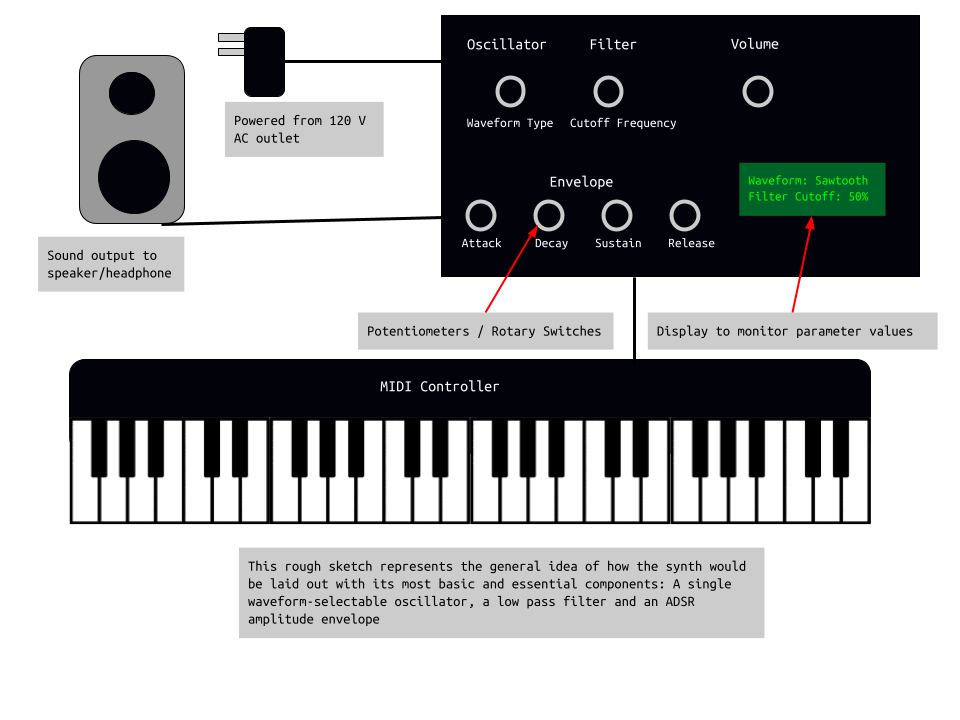
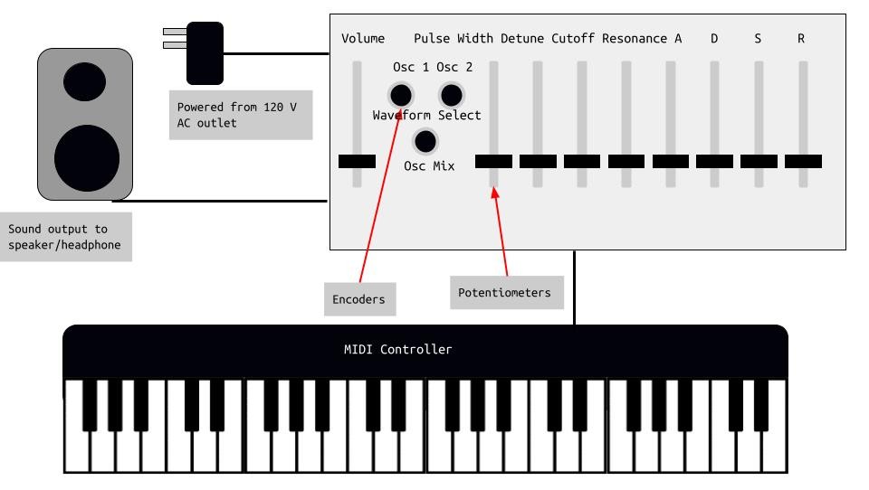
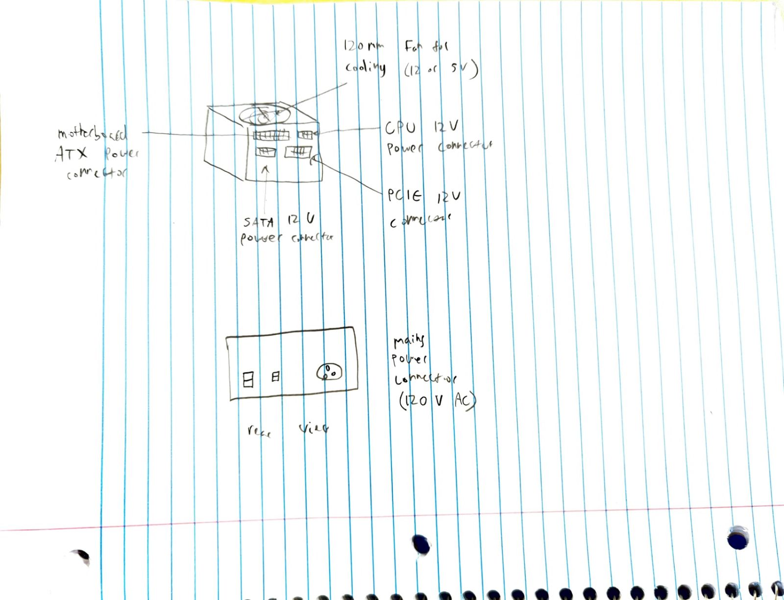
This is an updated sketch of what the Synthesizer project will look like in its completion at the end of Spring 2025. It will most likely be a standalone module controlled by a seperate MIDI keyboard. The controls on the front panel will be for waveform selection, filter cutoff, and the envelope parameters. There may also be a display of some sort to show current parameter values. The main output of the synth will be line level audio to be sent to speakers or headphones.
Next week, my tasks will be:
- Finish building new prototype electronics for DSP based synth using audio shield for Teensy
- Begin testing of updated DSP designs for oscillators, filters, and envelopes
- Begin testing designs for physical user controls (wiring and implementing code for potentiometers)
Fall 2024
Week of September 23:
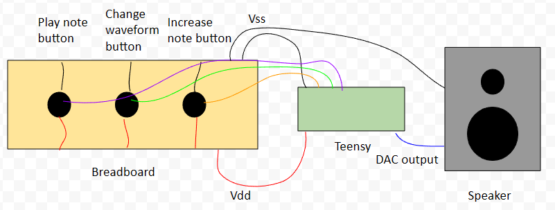
This week I made progress with generating the base waveforms on the Teensy 3.2 by using the IntervalTimer library, which helps with easily creating ISR’s that can be set to timeout to fractions of a microsecond (allegedly). This allowed for percise generation of waveforms at specific frequencies, from 0 to about 1200 Hz before the frequency stopped increasing correctly. I’m not sure what is causing this and will have to look into it more. I also added the ability to generate three different waveforms: sawtooth, square and triangle. I built a test board with push buttons to increase the note by a half step, change waveform, and turn the note on or off and wired the DAC output to a speaker and the oscilloscope to confirm functionality of adjusting pitch and waveform in real time, which will be useful for a CDR demo. A sketch of what the test board looks like:
I also spent some time compiling what I have designed/built/researched so far into slides for CDR.
Next week, my tasks will be:
- Order Teensy 4.1 and if it comes in see if having the higher timer frequency fixes the issue of >1200 Hz not being able to be generated with IntervalTimer
- Try to implement new DAC instead of using the onboard one on the Teensy
- Look into possible implementations for the filter IC
- Add functionality for changing the note frequency based on MIDI data for when Ian and Dylan get MIDI working
Week of September 16:
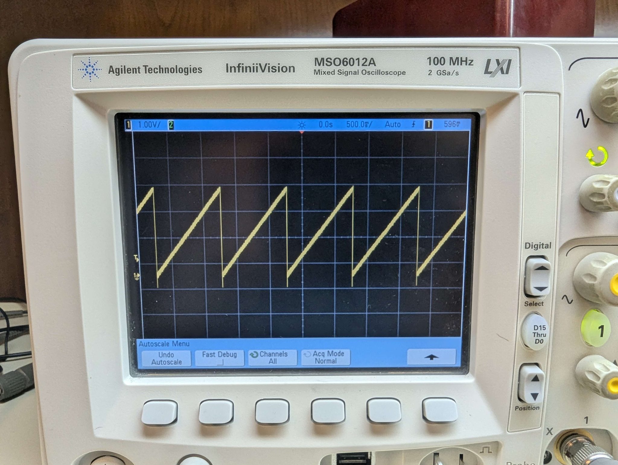
This week I switched from focusing on trying to implement software onto an arduino and instead a Teensy 3.2, since going with a Teensy will probably be more suitable for the project given its much higher clock speed and extensive audio synthesis functionality. I was able to get the Teensyduino plugin working in the Ardunio IDE and write some embedded software to generate a low frequency sawtooth wave using the Teensy’s built in DAC as a proof of concept for using the Teensy as a base waveform generator:
The main roadblock right now is with the current code I have running on the Teensy, generating higher frequency audio-spectrum waveforms is not reliable or even possible at frequencies higher than about 50 Hz. This is possibly because of the limitations of the built-in DAC or because of how the code is reading core clocks to generate steps in the function.
Next week, my steps will be:
- Investigate the root of the issue of reliably generating higher-frequency waveforms
- Create code for generating the other base waveforms the synth should be able to generate
- If the new DAC arrives, try to implement it on the Teensy
Week of September 9:
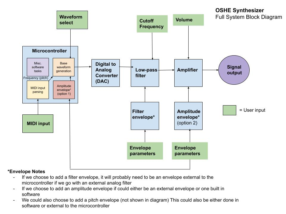
This week I created a tentative full system block diagram of the synthesizer to help the team understand better how the subsystems of the synth are connected:
I also began writing pseudocode for potential methods of digitally generating the synth’s base waveforms on a microcontroller, as well as researching how to implment this functionality onto an arduino using built-in hardware timers.
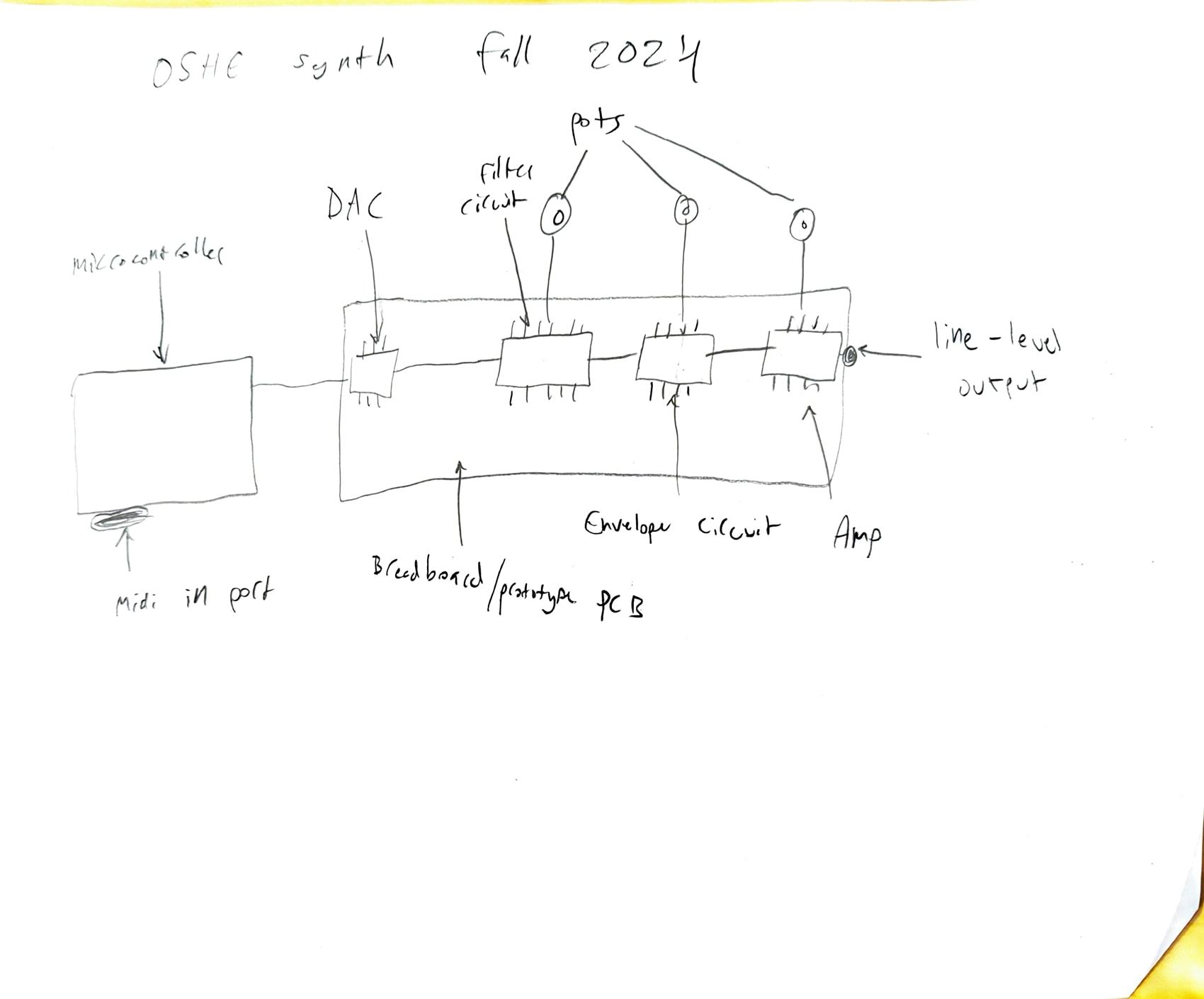
A sketch of what I think the project could look like at the end of the semester:
To-do list for upcoming week:
- Decide on analog filter chip to use
- Decide on DAC chip to use
- Implement waveform generation on arduino
Previous Semesters:
Week of September 11:
- Researched ATX Power Supply DC-DC conversion methods
- Researched Buck converter options
- Familarized with SPICE simulations
Week of September 18:
- Researched appropriate power factor for U.S. mains simulation
- Researced options for IC controller for DC/DC conversions
Week of October 1:
- Researched options for stepping down high voltage DC to usable DC
- Researched options for LLC DC step down converter
- Analyzed capacitance and inductance values on a physical power supply
Week of October 22:
- Researched design considerations for DC-DC Buck Converters
- Begin calculating component values for Buck Converters
- researched options for 12 V inversion IC
Week of October 30:
- Aquired test computer system for future power supply testing
- Researched TI Buck controller IC options
Week of January 21:
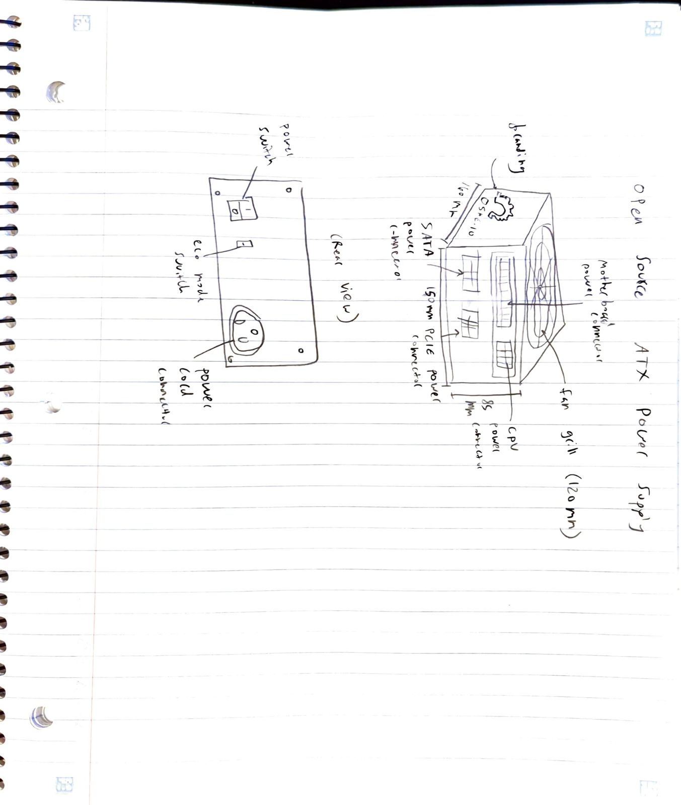
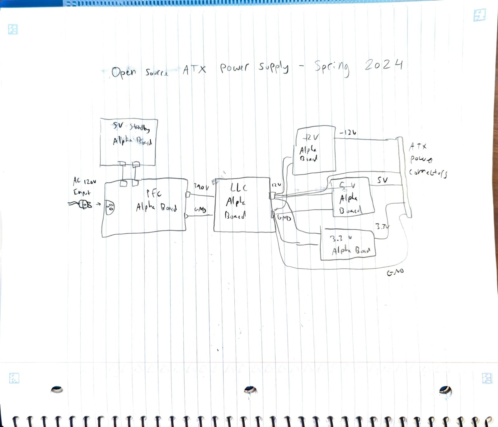
- Sketch of final ATX Power Supply design
Next week tasks:
- Finalize IC choice for 3.3 V Buck converter
- Finalize IC choice for 5 V Buck converterv
- Investigate options for 12 to -12 V converstion topology
Week of January 28:
- Narrowed down IC choice for 3.3 V and 5 V buck converter
- Chose IC from narrowed down options
- Researched options for using buck converter for -12 V conversion
Next Week’s Tasks:
- Begin schematic design for 5 V buck
- Choose buck converter for -12 V conversion
Week of February 4:
- Learned how to load schematics into KiCad for 5 V buck converter
- Researched requirments for -12 V buck converter
Next Week:
- Finish Schematic loading for 5V buck converter
- choose IC for -12 V buck converter
Week of February 11:
- Schematic Design for 5V buck converter
- Load Schematic for 3.3 V buck converter into KiCad
Next Week:
- Finish Schematic Loading for 3.3 V Buck Converter
- Finish Schematic design for 5 V buck converter
Week of February 18:
Project Progress:
- Reviewed schematic for 5 V DC/DC Buck converter
- Reviewed schematic for 3.3 V DC/DC Buck converter
Next Week:
- component selection for 5 V DC/DC breakout
Week of March 3:
- Finished KiCad Schematic for 5 V DC/DC conversion
- New selection for 5 V buck converter chip
Next Week:
- New selection for 3.3 V buck converter chip
- Finish KiCad schematic for 3.3 V DC/DC conversion
Week of March 10:
- Finished KiCad Schematic of 3.3 V DC/DC conversion
- completed schematic review documents for 5 V and 3.3 V circuits
Next Week:
- BOM creation for 5 V components
- BOM creation for 3.3 V components
Week of March 17:
- Footprint importing for 5 V schematic
- Footprint important for 3.3 V schematic
Next Week:
- PCB layout finished for 5 V schematic
- PCB layout finished for 3.3 V schematic
Week of March 24:
- PCB general component layout for 3.3 V alpha board
- PCB trace routing begun for 3.3 V alpha board
Sketch of current design for end of Spring 2024 Semester:
- The design has changed considerably from the original as we are now not going to be making the first prototype in the ATX form factor but rather in individual alpha PCBs of each subsystem to make integration and testing less formidable. Each board will be connected to the next board in the conversion process via terminals and there will be several test points to test functionality once assembly is complete.
Next Week:
- PCB layout for 5V board complete
- Order components from BOM for 3.3 V and 5 V boards
Week of March 31:
- Worked on trace placement for 3.3 V PCB
- Worked on general component layout of 5 V PCB
Next Week:
- Begin compiling documentation for 5 V and 3.3 V conversion circuits for final report
- Begin comiling documentation for planned testing suite for hardware once assembled
Week of April 7:
- Worked on documentation for methodolgy and characterization of 5 and 3.3 V converters
- Worked on documentation for the planned tests that will be conducted on the boards once assembled
Next Week:
- Complete PCB layouts for 5 and 3.3 V PCBs complete
- Finish documentation for 5 and 3.3 V converters for final report
- Finalize project check off demonstration procedures
Week of April 14:
- Finished Documentation for 5 and 3.3 V converters for final report
- Prepare for project spec rundown on Tuesday
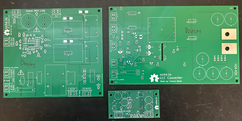
- Image of completed AC/DC boards:
Next Week:
- Any further preperations for project spec rundown before Tuesday
- Project spec rundown on Tuesday