
Week of 9/17/2023
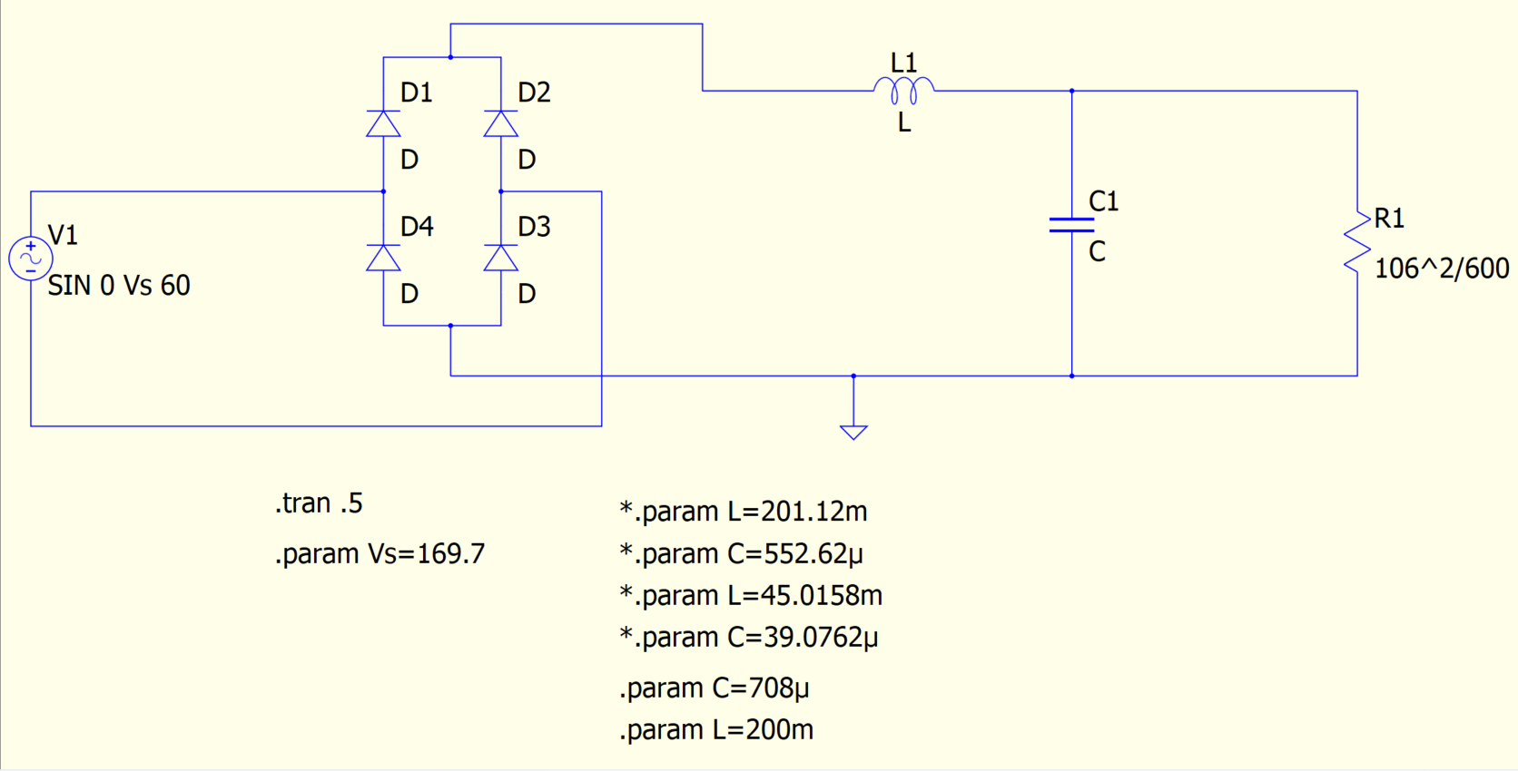
This week I have been looking into passive vs. active power factor correction (PFC) to learn which would be a more viable option for our project. Passive PFC won for its simplicity in footprint, circuit design, and decreased cost. The second part which has been my main focus was designing the output filter for our rectifier. This is being done by assuming a perfect AC input with zero noise which will then be incorporated and tweaked to match performance with the filtered input from mains and the buck converter to step our DC voltage down to the 12V, 5V, and 3.3V rails we need. The design has landed on an LC filter to rectify the voltage. The best performing circuit I have found so far has a ripple voltage of ~1.7%. Adding second inductor further improves upon the smoothing but the planned converter to step down to an input voltage for our regulators will also effect the ripple voltage so that will need to be implemented into the simulation before final tuning is done.
Week of 9/24/2023
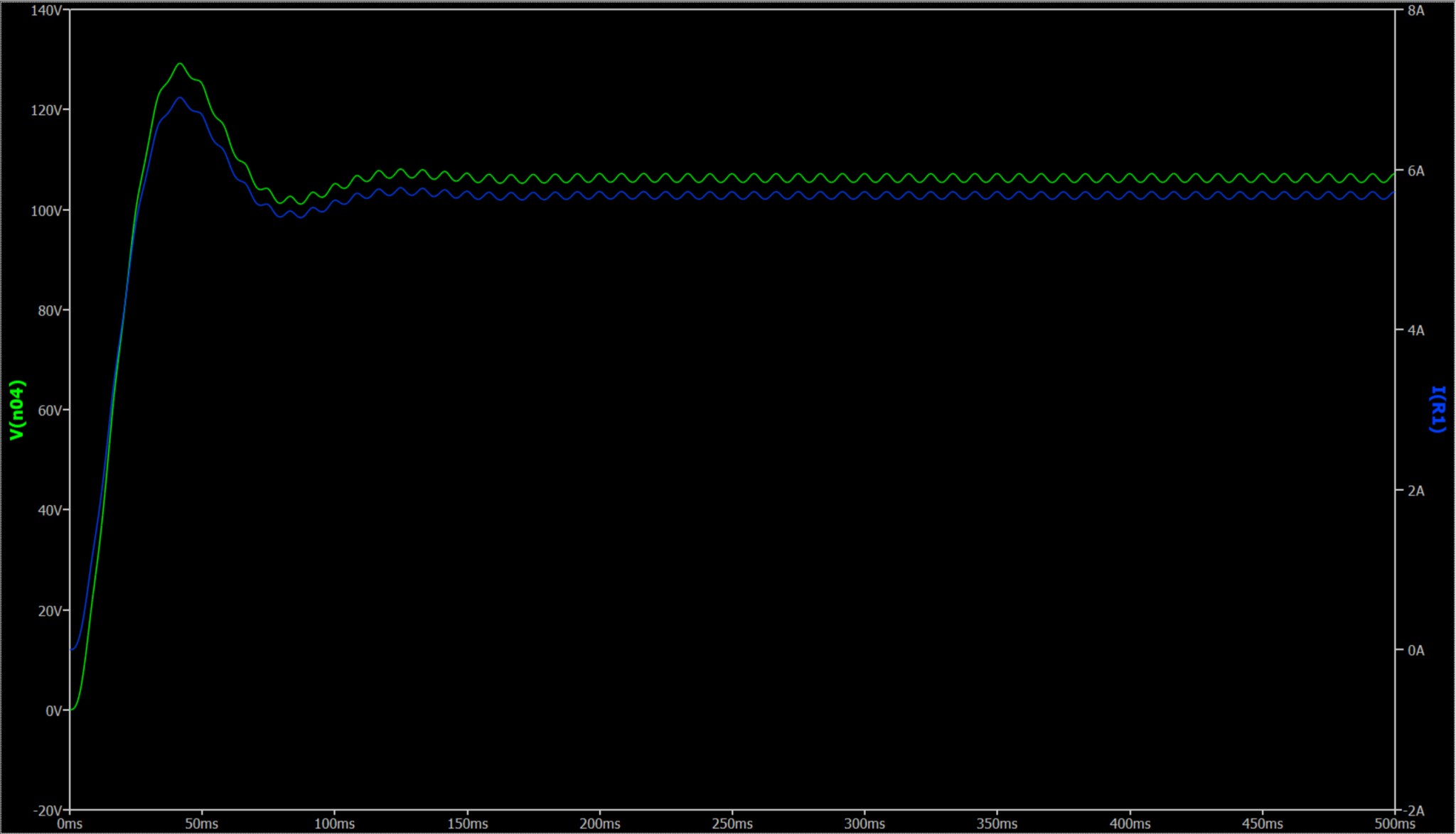
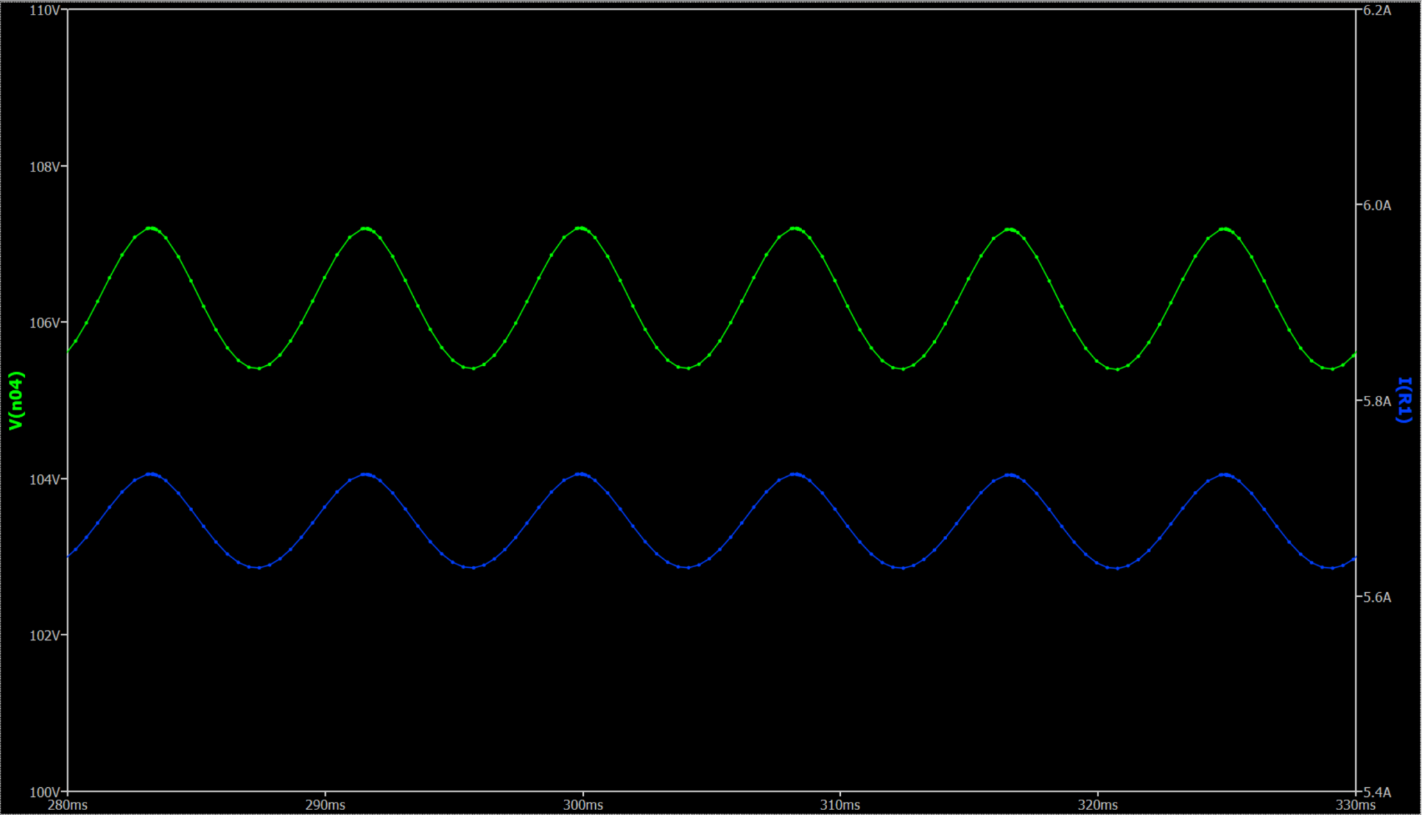
This week the mains input simulation with clipping was finished so it was added to the rectifier filter simulation and the filter didn’t perform near expected response. Along with that, real component values are being considered for parts ordering and the previous component values found are unrealistic for our use case. Different filters are going to be considered again with a Pi filter looking promising and our expectations of the filter’s output are going to be re-evaluated to help with finding what an acceptable amount of ripple voltage at this stage will be.
Week of 10/1/2023
Discovered that the filter was violating KVL so switched back to an LC filter and then figured out the correct way to solve for component values after discussing with one of my professors. The values were still too high so I did some more digging for a reference design on an AC/DC converter and found a 500W reference design that we could use to base our general schematic upon as well as minimum component calculations. Within that I discovered the inductors within the Active PFC block we are going to use replace the inductor in my filter design so I am shifting to help with both PFC design and Flyback simulation.
Week of 10/8/2023
The main focus for this week was working on our Critical Design Review. The rest of our time was spent focusing on our IC selection for the PFC and LLC converter topologies.
Week of 10/15/2023
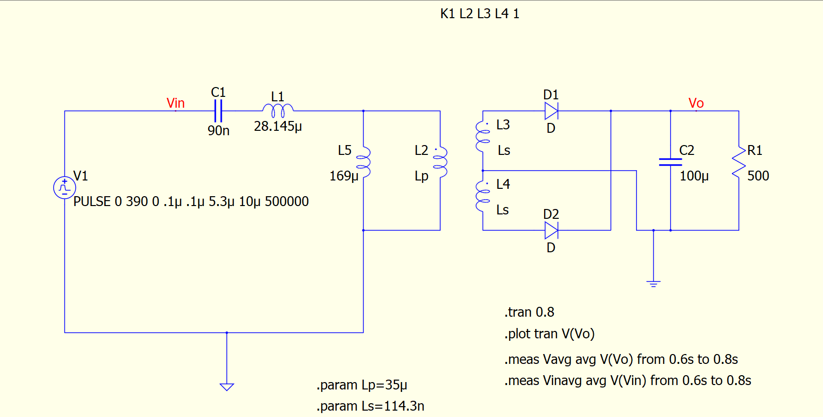
Efforts put into verifying compatibility between both IC’s. Providing power to both IC’s during startup and steady state looked into within this effort as well. I have started working on an LLC simulation to verify my own understanding of the theoretical operation of this topology. Some “too small of timestep” issues being encountered while switching the high and low FETs at high frequencies around 500kHz so a square wave output is being used in place of the FETs to function as an ideal square wave input of the LLC converter. This will allow the topology to be tested so it can be partially ruled out as part of the issue.
Week of 10/22/2023
Main focus was getting a working LLC converter simulation with realistic components. Some issues were coming up with a “too small of time step” error so I simplified the input by removing the FETs and using an ideal square wave source to get the LLC topology to output the correct value. Then adding the FETs back in there is no more time step issue but the output is in the pV to nV range so I am looking into the control circuits for the FETs. Open-loop controls are being used here so some issues are expected. Trying to add a closed loop control topology might be valuable but the benefits will have to be weighed against the added time to get the simulation functional.
Week of 10/29/2023
Work has started on capturing the full schematics for the rectification, power factor correction, and LLC topologies. KiCAD will be used for schematic and PCB layout work.
Week of 11/5/2023
The schematic for the LLC topology was completed. The switching simulation for the LLC is still having issues, the main issue being focused on is the switching of the FETs with some interaction there most likely causing the sim to not behave as intended. I have explored using real vs ideal FETs and adding resistors to the driving topology to prevent a short somewhere in the system. We are having trouble in our early searches for an LLC Resonant transformers that is rated for 600W.
Week of 11/12/2023
I have checked many vendors for LLC Resonant converters but the best ones I can find are rated for a max of 250W. After talking to our company sponsor contact and a professor I have some new parameters to search using and looking into custom magnetics might be our best option.
Week of 11/26/2023 – End of Fall 2023
After searching during our Thanksgiving break and discussing further, Finding a ferrous core online and designing our own might be another option but not as desirable as consistency and accuracy is an issue when winding inductors by hand. Next steps are to get into contact with suppliers and see if they have something available that we could purchase at a reasonable price and quantity with the specifications we are looking for.
ATX Power Supply Spring 2024
Week of 1/21/2024
Our goal for the end of the semester is to have 3 functional Evaluation PCB’s, 1 Rectification and PFC board, 1 LLC board, and 1 Buck converter board. This will allow us to have easier access to test points, quicker rework times, and more space to layout components without worrying about space constraints and thermal considerations. This will also allow us to do the PCB layout and PCBA solder work in parallel.
This week I finalized my calculations for an ideal LLC transformer and talked with Wurth Electronik but they do not have a component that meets our requirements so a different path will have to be taken to keep us on track.
My goals next week are to get into contact with one more company for custom magnetics and in parallel complete all of the necessary calculations for winding our own inductor. Following an Infineon Application note where they wound their own LLC transformer for a 600W server power supply, it will help to decrease the burden of finding the right equations while also providing a good example. The parameters that need to be calculated/confirmed are wire diameter, primary, secondary, and auxiliary inductances, # of turns for each coil, and accounting for power loss via magnetics and (I^2)R losses. I suspect that making our own transformer will be the path that I will have to take.
My biggest concerns for next week are encountering any issues with my calculations and suppliers not having the correct materials that we need for a reasonable price.
Week of 1/28/2024
I was not able to get into contact with a company for custom magnetics so that path is being shelved. I was able to complete some calculations for winding our own transformer so I plan to put together the parts list for the Litz wire, core, and bobbin this coming week and order it to start building as soon as possible. Some further exploration into my transformer calculations will be done while waiting for parts to make sure nothing is overlooked. Aside from that, I plan to start working on passive selection for components that are not reliant upon the transformer and back feed my calculations of the theoretical transformer into my full LLC calculator to get closer to the final values needed for passives. Final selection will not be made though until I have made the core and know its true inductance.
Week of 2/4/2024
This week I have completed the necessary calculations for the construction of my transformer and have put together a list of parts to order early next week so we can begin construction. My goal for next week is to get the parts ordered, finish any extra calculations, and begin sizing passive components while I wait for parts to come in.
Week of 2/11/2024
This week I have ordered the parts for the transformer and have already received the cores, bobbins, and copper band. The table below contains the parts and their prices. I planned for some spares and the roll of wire has enough to wind 10 transformers. The total cost ended up around the final cost of three LLC transformers from a manufacturer.
| Price | Name | Unit Price | Qty | Total Cost | Supplier |
| Magnetic Core | PQ35/35-3F36 | 5.98 | 3 | 17.94 | Digi-Key (Ferroxcube) |
| Litz Wire 2oz/39′ | 20AWG, 64/38 Stranding | 24.14 | 1 | 24.14 | Remington Industries |
| Bobbin | CPV-PQ35/35-1S-12P-Z | 2.23 | 3 | 6.69 | Digi-key(Ferroxcube) |
| Copper Band | Copper Sheet Roll 1000mm x 20mm x 0.5mm | 12.49 | 1 | 12.49 | Amazon (uxcell) |
| 61.26 |
I have started working on passives selection and plan to get as much of that done between CDR work so we can start on PCB layout when we return from spring break. Next week will have some scheduling conflicts with homework and lab reports due next week so I am expecting some of the passive component selection to bleed into spring break. I also need to start building the transformer so I can feed the final inductance values back into my calculator for to get the capacitor network selected but I will be able to find some estimated values and get their package sizes so layout should not be hindered by those unknown component values.
Week of 2/18/2024
This week I have presented my CDR presentation with our group and fielded feedback from other team members on the enterprise. I have been continuing work on passive selection and since all of the parts for my transformer have arrived, I will begin winding my transformer when I return from spring break. The Litz wire that I received is a twisted bundle of individually insulated wires without a second coating of insulation. This will pose an interesting issue for winding and rewinding when I go back through and apply the final potting material while keeping the strands from untwisting themselves. I see this as being my largest issue in the coming weeks as long as passive selection doesn’t encounter any issues.
Week of 3/3/2024
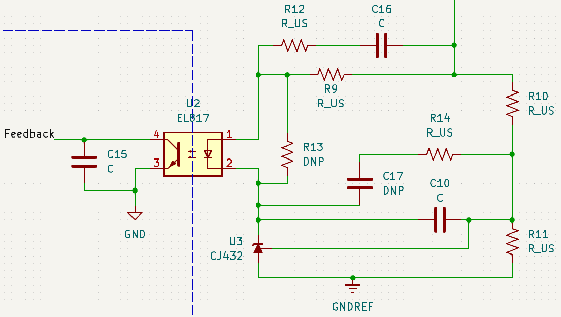
This week I have been working on passive selection for the various resistors and capacitors required for the LLC sub-system. Many of the components are chosen using the provided TI calculator for the IC that was chosen. The final components that are still giving me some problems are those for the feedback circuit that utilizes the optoisolator to cross the isolation barrier between the high voltage side and the output side, and the bulk capacitors for the 12V output. Correctly setting the voltage divider for the shunt voltage regulator is very important and I have an initial guess at the circuit worked out. The resistor network along with the RC compensation components will most likely need to be corrected once we have the board manufactured and are testing it. There will be other pads for additional components that will not be pre populated so we can add other components ot meet required values or make bias adjustments.
Selecting the output capacitors is difficult because the output RMS currents we need to meet is around 24A at the resonant frequency of 100kHz. Dividing up this current requirement across multiple parallel capacitors is the best path to follow but the high current requirement still pushes us towards very expensive capacitors. I will be double checking my calculations to make sure this value is correct and exploring other types of capacitors outside of electrolytics to see if I can find a different type that will work better for our power requirements.
Next week will be setting up documentation for a schematic review with our sponsor as we go into PCB layout. This will help us catch issues before we enter layout and have to back track.
Week of 3/10/2024
The schematic review is mostly done for the LLC subsystem. Some catch up work will be done before Monday to have it ready for review. Steps for next week are starting PCB layout. I plan to get the general board dimensions and zones laid out on the sheet to try and find any early spacing issues and try to set an isolation barrier with a keep out zone on both copper layers. A board cutout beneath the optoisolator may also be added to make sure no copper traces can connect across the isolation barrier. Some issues that I could see arising is changes to the schematic and time conflicts as I prepare for two exams this week.
Week of 3/17/2024
We have completed the schematic review and are now waiting for feedback from our sponsor. Provided is the final schematic before review confirmation for the LLC. While we wait we will be assuming that there are no issues and begin working on the PCB layouts. As we enter PCB layout we are starting to consider PCB stack-up with layer count and power planes if we go for a stack-up with more than two layers. Goals for the end of this week is to have the components placed in their approximate final positions with traces routed for either the power or signal paths.
Week of 3/24/2024
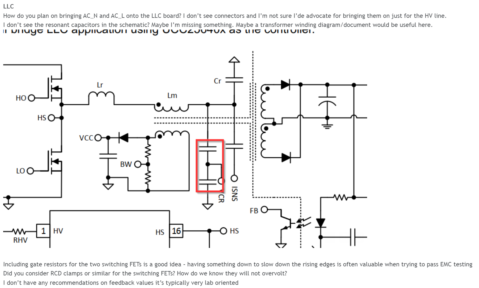
This week we have been working on the PCB layouts for our subsystems assuming that there were no issues with our schematics and that everything was perfect. We received our schematic review feedback from our company sponsor with issues regarding our schematics and problems we should address, both general issues with our schematics and specific issues with each circuit design. Most of the general feedback was just schematic hygiene such as having grounds all point down and making sure the text is readable. The feedback on the LLC schematic can be seen below.
The goal this week is to review and address our feedback, finish and review our PCB layouts for significant errors, and order boards early next week along with passives for assembly. Also shown below is the current state of the layout. Some Issues still need to be addressed which were brought up verbally such as moving to a 4-layer board from a two layer board so we can have full pours for the high power connections. The Gate resistors, RCD clamps to protect overvolting our FETs, and some mounting holes to add nonconducting standoffs still need to be done but should not produce major changes to the board layout. Effort will be put forth to compact the design by placing any low power signal traces on the inner layers so components can be placed closer together.
General EMC considerations are being followed on this design to improve operation such as placing decoupling capacitors as close to the desired components as possible but since this is mostly for validating the circuit design and component selections, passing EMC requirements is not a goal for this build.
Week of 4/6/2024
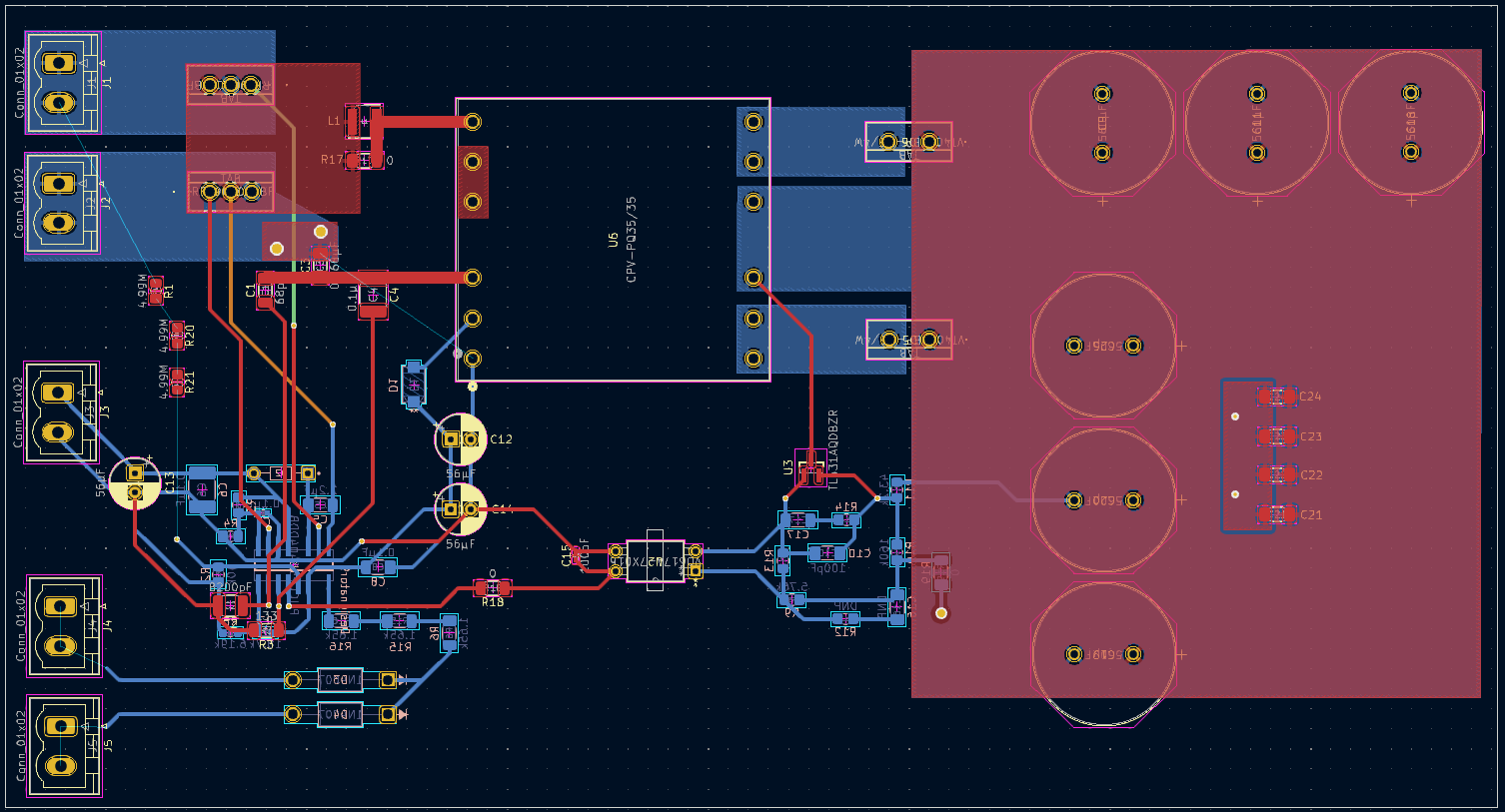
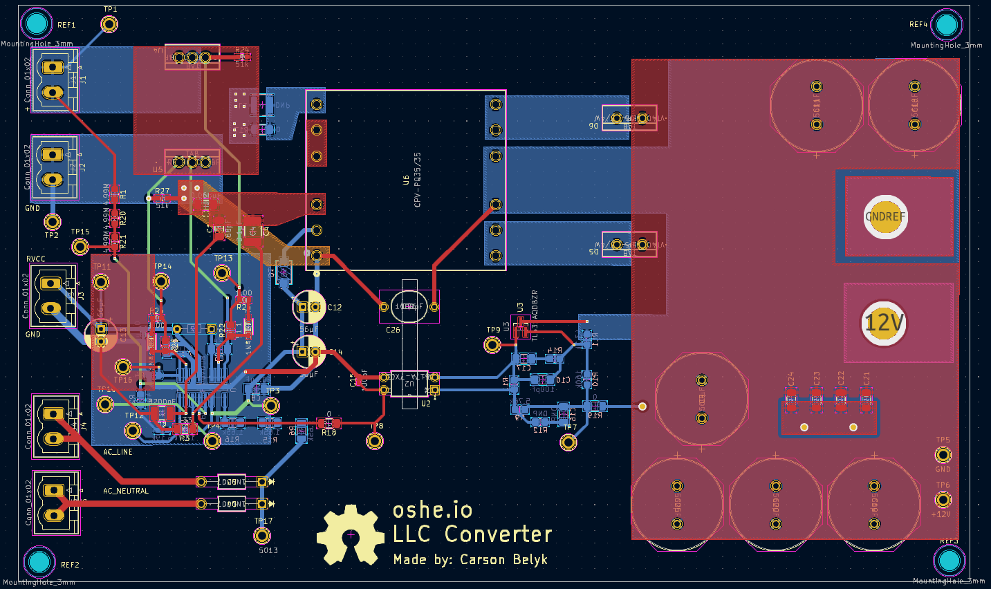
This week we finalized our PCB layouts making changes recommended by our sponsor. Adding test points, converting some traces to pours, mechanical mounting points, and adding pads for output terminal lugs. I had to create some custom exposed pads for the output connections and account for space to add heatsinks to the MOSFETs and High power diode packs. 2oz copper is used for the outer layers as those are mostly switching power nets and are also pours to increase heat dissipation. The inner layers are a 0.5oz copper and only signal layers for the FET gates and auxiliary connection to GND. Many test point footprints were also added so we could add loop test points for easier testing and verification of design goals being met. After making those changes, we went over our boards again with our sponsor and ordered them from JLCPCB as well as components for our boards on Digi key. Below is the final PCB layout for the LLC Alpha Board that we ordered.
Goals for next week are to work on the transformer and get it wound as well as working on the educational documentation for my subsystem.
Week of 4/7/2024
This week while we have been waiting on parts, we have been working on our educational documentation. The goal of this documentation is to explain how each of our subsystems operate and the design choices we made to create them.
Goals for next week are to continue working on the educational documentation until our boards come in. If our boards come in early enough, we plan to solder components to our boards and begin some characterization testing given we have enough time and don’t encounter any issues.
Week of 4/14/2024 – End of Spring 2024
We have wrapped up work on our educational documentation and only have our semester report left to complete. We did receive our boards but didn’t have enough time in our schedules to assemble them because we don’t want to rush this stage of the process. Our plan is to assemble the boards next semester and test them so there is less of a chance that we make a mistake and destroy some of our components or the boards themselves. Personal safety is also a big concern since we will be playing with utility mains voltage so we want to verify that we have accounted for as many potential issues as we can before applying power. This will help decrease the chance of blowing a breaker, fuse, or possibly shocking ourselves or someone else.
We feel this is in a good state currently for next semester to assemble our alpha boards, go thorough test verification, resolve any circuitry issues that we find from these tests, and combine into a final PCB that complies with the ATX form factor for a version 1.0.
Week of 9/8/2024
The final product look has not changed much with the final design to look like this
For the two weeks before this, I have been working to populate my Alpha board with components and winding my transformer. The board was fully populated and short tested with no visible assembly issues. This was aided by use of the plexus makerspace air solder dispensing tool and reflow oven for SMD components.
In between this work, I wound one transformer and took inductance measurements to find the magnetizing and leakage inductance. Due to poor construction quality, the values were not close to the desired and couldn’t be tuned to work. Therefore a second transformer was wound, using one continuous strip for the secondary inductor and ensuring that it was as tight and consistent as I could wind it by hand. This time the magnetizing inductance could be tuned by increasing the air gap of the core using paper to separate both halves. This allowed the magnetizing inductance to be tuned but the leakage was still a bit large.
Knowing that the resonant circuit likely won’t function properly, I decided to still solder the transformer on and supply power to the board to find potential issues. Nothing happened but the output voltage was not correct so some components will need to change to adjust for the real transformer values.
My To-Do list for next week is as follows
- Order new resonant capacitors
- Redesign the feedback circuit and order new components if needed
- Populate and test 5V Standby circuit (if time is available)
One concern that I have is the feedback circuit taking a long time to redesign and not working as intended. Luckily I am able to isolate the feedback loop and power it separately from the main power stage with 0Ohm resistors, allowing my feedback loop to be tested without providing high power to the main power path.
Week of 9/15/2024
This week I ordered new parts for my feedback circuit, new resonant capacitors, and other various components. While waiting for the parts to come in, I assembled and tested the 5V Standby board. The board wasn’t working properly and as we were trying to diagnose the issue, a passive failed. My parts arrived the next day so I replaced the old components with the new ones, starting with the resonant capacitors, and the board started to deliver power to the output. I assumed the feedback was not functioning properly so I replaced those components and plan to test it Monday.
Next Week To-Do List
- Test the LLC Board with the Evaluation and custom PFC boards
- Debug issues that may arise
- Talk with EERC Laboratory and Safety advisors about setting up full load testing
- Begin schematic and layout consolidation for the final product
- Start working on CDR slideshow (lowest priority)
The biggest concern I have about next week is my LLC board still having issues. That would currently be the largest blocker to significant forward progress. If there are issues, the first area I will look at is the resonant circuit and then the feedback circuit. The feedback circuit will take a long time to debug and push me back significantly.
Week of 9/22/2024
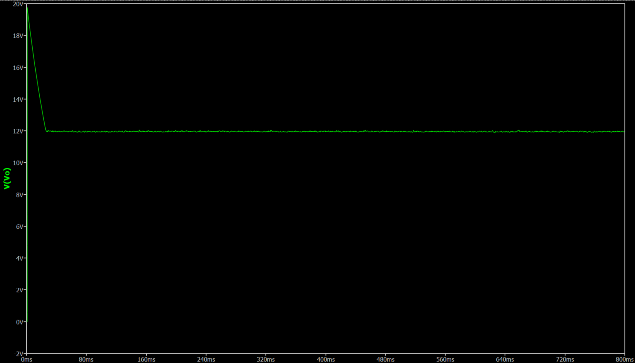
We tested the board on Monday and it still wasn’t working as intended. Looking over my schematic and comparing with my design calculator, I found that one of my sense capacitors was a factor of 1000 too large so that component was replaced along with the further down resistor and a capacitor was stacked on top of the resistor to properly set the voltage divider. The bias winding voltage sense divider was also found to have incorrect values and in the wrong location post-rectification instead of pre-rectification so those issues were also fixed which corrected those voltage readouts.
Upon further testing, it was found that RVCC was not the correct voltage so investigation into that issue has begun and it is believed that this is the last issue that is preventing proper operation. To fix this issue, the THT capacitor will be replaced with ceramics as I believe it is both too large and the electrolytic has a notable impedance at 100kHz that could be loading the internal LDO too much.
The PFC and LLC schematics were combined and blocked into “rooms” to simplify later documentation and PCB layout efforts. Component value and package size changes still need to be updated from the LLC debug effort.
Next Week To-Do List
- Replace RVCC electrolytic with a ceramic capacitor
- Work on CDR Slides
- Continue to work on combined schematics and add the new component changes
- Debug any further issues that arise
The main concerns I have are the RVCC cap change does not fix the board or there are other issues. Otherwise I have no other concerns for next week.